- 您现在的位置:买卖IC网 > PDF目录8607 > LTC6405CMS8E#PBF (Linear Technology)IC AMP/DRVR DIFF R-R 5V 8-MSOP PDF资料下载
参数资料
| 型号: | LTC6405CMS8E#PBF |
| 厂商: | Linear Technology |
| 文件页数: | 13/26页 |
| 文件大小: | 0K |
| 描述: | IC AMP/DRVR DIFF R-R 5V 8-MSOP |
| 标准包装: | 50 |
| 类型: | ADC 驱动器 |
| 应用: | 数据采集 |
| 安装类型: | 表面贴装 |
| 封装/外壳: | 8-TSSOP,8-MSOP(0.118",3.00mm 宽)裸露焊盘 |
| 供应商设备封装: | 8-MSOP-EP |
| 包装: | 管件 |
| 产品目录页面: | 1323 (CN2011-ZH PDF) |

LTC6405
20
6405fb
For more information www.linear.com/6405
applications inForMation
TheLTC6405’sinputreferredvoltagenoisecontributesthe
equivalent noise of a 155Ω resistor. When the feedback
network is comprised of resistors whose values are less
than this, the LTC6405’s output noise is voltage noise
dominant (see Figure 11):
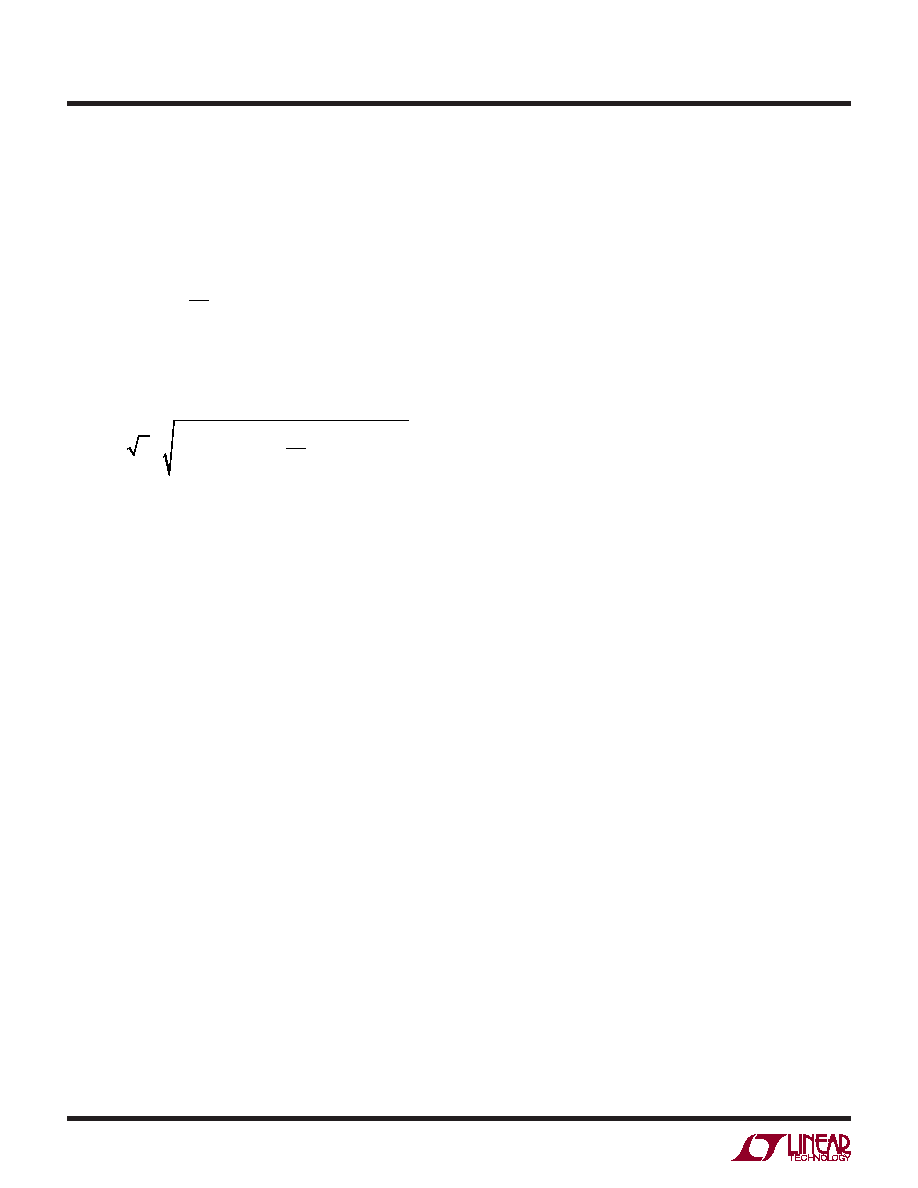
eno ≈eni 1+
RF
RI
Feedback networks consisting of resistors with values
greater than about 200Ω will result in output noise which
is resistor noise and amplifier current noise dominant.
eno ≈ 2 In RF
(
)2 + 1+ RF
RI
4 k T RF
Lowerresistorvalues(<100Ω)alwaysresultinlowernoise
at the penalty of increased distortion due to increased
loading of the feedback network on the output. Higher
resistor values (but still less than <500Ω) will result in
higher output noise, but typically improved distortion due
to less loading on the output. The optimal feedback resis-
tance for the LTC6405 runs in between 100Ω to 500Ω.
The differential filtered outputs +OUTF and –OUTF will
have a little higher noise than the unfiltered outputs (due
to the two 50Ω resistors which contribute 0.9nV/√Hz
each), but can provide superior signal-to-noise due to the
output noise filtering.
Layout Considerations
Because the LTC6405 is a very high speed amplifier, it is
sensitive to both stray capacitance and stray inductance.
In the QFN package, three pairs of power supply pins are
provided to keep the power supply inductance as low
as possible to prevent any degradation of amplifier 2nd
harmonic performance. It is critical that close attention be
paid to supply bypassing. For single supply applications
it is recommended that high quality 0.1F surface mount
ceramic bypass capacitor be placed directly between each
V+ and V– pin with direct short connections. The V– pins
should be tied directly to a low impedance ground plane
with minimal routing. For dual (split) power supplies, it is
recommended that additional high quality, 0.1F ceramic
capacitors are used to bypass V+ to ground and V– to
ground, again with minimal routing. For driving large
loads (<200Ω), additional bypass capacitance may be
needed for optimal performance. Keep in mind that small
geometry (e.g., 0603) surface mount ceramic capacitors
haveamuchhigherselfresonantfrequencythandoleaded
capacitors, and perform best in high speed applications.
Anystrayparasiticcapacitancestogroundatthesumming
junctions,+INand–IN,shouldbeminimized.Thisbecomes
especially true when the feedback resistor network uses
resistor values >500Ω in circuits with RF=RI.Alwayskeep
in mind the differential nature of the LTC6405, and that it
is critical that the load impedances seen by both outputs
(stray or intended), should be as balanced and symmetric
as possible. This will help preserve the natural balance
of the LTC6405, which minimizes the generation of even
order harmonics, and improves the rejection of common
mode signals and noise.
It is highly recommended that the VOCM pin be bypassed
to ground with a high quality ceramic capacitor whose
value exceeds 0.01F. This will help stabilize the common
mode feedback loop as well as prevent thermal noise from
the internal voltage divider and other external sources of
noise from being converted to differential noise due to
divider mismatches in the feedback networks. It is also
recommended that the resistive feedback networks be
comprised of 1% resistors (or better) to enhance the
output common mode rejection. This will also prevent
VOCM input referred common mode noise of the common
mode amplifier path (which cannot be filtered) from being
converted to differential noise, degrading the differential
noise performance.
Feedback factor mismatch has a weak effect on distortion.
Using 1% or better resistors will limit any mismatch from
impacting amplifier linearity. However, in single supply
level shifting applications where there is a voltage differ-
ence between the input common mode voltage and the
output common mode voltage, resistor mismatch can
make the apparent voltage offset of the amplifier appear
worse than specified.
相关PDF资料 |
PDF描述 |
|---|---|
| SY88843VMG | IC AMP LIMIT CML TTL SD 16MLF |
| VE-2TM-IV-F1 | CONVERTER MOD DC/DC 10V 150W |
| AD8307ARZ-RL7 | IC AMP LOGARITHMIC 8-SOIC |
| AD5678BRUZ-1REEL7 | IC DAC 12/16BIT SPI/SRL 14TSSOP |
| VE-2T1-IV-F4 | CONVERTER MOD DC/DC 12V 150W |
相关代理商/技术参数 |
参数描述 |
|---|---|
| LTC6405CMS8E-TRPBF | 制造商:LINER 制造商全称:Linear Technology 功能描述:2.7GHz, 5V, Low Noise, Rail-to-Rail Input Differential Amplifi er/Driver |
| LTC6405CUD | 制造商:Linear Technology 功能描述:DIFF AMP 5V 2.7GHZ R/R 16QFN 制造商:Linear Technology 功能描述:DIFF AMP, 5V, 2.7GHZ, R/R, 16QFN |
| LTC6405CUD#PBF | 功能描述:IC DIFF AMP/DRIVER R-R 16-QFN RoHS:是 类别:集成电路 (IC) >> 线性 - 放大器 - 专用 系列:- 产品培训模块:Lead (SnPb) Finish for COTS Obsolescence Mitigation Program 标准包装:60 系列:- 类型:可变增益放大器 应用:CATV 安装类型:表面贴装 封装/外壳:20-WQFN 裸露焊盘 供应商设备封装:20-TQFN-EP(5x5) 包装:托盘 |
| LTC6405CUD#TR | 制造商:Linear Technology 功能描述:DIFF-AMPLIFIER, 2.7GHZ, 690V/US, QFN-16, No. of Amplifiers:1, Input Offset Voltage:6mV, Bandwidth:2.7GHz, Amplifier Case Style:QFN, No. of Pins:16, Supply Voltage Range:4.5V to 5.25V, Slew Rate:690V/s, Supply Current:18mA, MSL:- , RoHS Compliant: No |
| LTC6405CUD#TRPBF | 功能描述:IC DIFF AMP/DRIVER R-R 16-QFN RoHS:是 类别:集成电路 (IC) >> 线性 - 放大器 - 专用 系列:- 产品培训模块:Lead (SnPb) Finish for COTS Obsolescence Mitigation Program 标准包装:60 系列:- 类型:可变增益放大器 应用:CATV 安装类型:表面贴装 封装/外壳:20-WQFN 裸露焊盘 供应商设备封装:20-TQFN-EP(5x5) 包装:托盘 |
发布紧急采购,3分钟左右您将得到回复。