- 您现在的位置:买卖IC网 > PDF目录67759 > LTC6405CMS8E#TRPBF (LINEAR TECHNOLOGY CORP) SPECIALTY ANALOG CIRCUIT, PDSO8 PDF资料下载
参数资料
| 型号: | LTC6405CMS8E#TRPBF |
| 厂商: | LINEAR TECHNOLOGY CORP |
| 元件分类: | 模拟信号调理 |
| 英文描述: | SPECIALTY ANALOG CIRCUIT, PDSO8 |
| 封装: | LEAD FREE, MSOP-8 |
| 文件页数: | 7/24页 |
| 文件大小: | 281K |
| 代理商: | LTC6405CMS8E#TRPBF |
LTC6405
15
6405fa
APPLICATIONS INFORMATION
General Amplier Applications
As levels of integration have increased and correspond-
ingly, system supply voltages decreased, there has been
a need for ADCs to process signals differentially in order
to maintain good signal to noise ratios. These ADCs are
typically supplied from a single supply voltage which can
be as low as 3V, and will have an optimal common mode
input range of 1.25V or 1.5V. The LTC6405 makes interfac-
ing to these ADCs easy, by providing both single-ended
to differential conversion as well as common mode level
shifting. The gain to VOUTDIFF from VINM and VINP is:
V
OUTDIFF = V
+OUT –V–OUT ≈
R
F
R
I
V
INP –VINM
()
Note from the above equation, the differential output volt-
age (V+OUT – V–OUT) is completely independent of input
and output common mode voltages, or the voltage at the
common mode pin. This makes the LTC6405 ideally suited
for pre-amplication, level shifting and conversion of single
ended signals to differential output signals in preparation
for driving differential input ADCs.
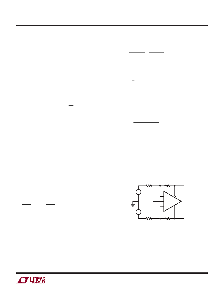
Effects of Resistor Pair Mismatch
Figure 3 shows a circuit diagram which takes into consid-
eration that real world resistors will not match perfectly.
Assuming innite open loop gain, the differential output
relationship is given by the equation:
V
OUTDIFF = V
+OUT –V–OUT
R
F
R
I
V
INDIFF +
Δβ
β
AVG
V
ICM –
Δβ
β
AVG
V
OCM
where:
RF is the average of RF1, and RF2, and RI is the average
of RI1, and RI2.
βAVG is dened as the average feedback factor from the
outputs to their respective inputs:
β
AVG =
1
2
R
I1
R
I1 + RF1
+
R
I2
R
I2 + RF2
Δ
β is dened as the difference in feedback factors:
Δβ =
R
I2
R
I2 + RF2
–
R
I1
R
I1 + RF1
VICM isdenedastheaverageofthetwoinputvoltagesVINP
and VINM (also called the input common mode voltage):
V
ICM =
1
2
V
INP + VINM
()
and VINDIFF is dened as the difference of the input voltages:
VINDIFF = VINP – VINM
VOCM is dened as the average of the two output voltages
V+OUT and V–OUT:
V
OCM =
V+OUT + VOUT
2
When the feedback ratios mismatch (Δ
β), common mode
to differential conversion occurs.
Setting the differential input to zero (VINDIFF = 0), the de-
gree of common mode to differential conversion is given
by the equation:
V
OUTDIFF = V
+OUT –V–OUT ≈ VICM –VOCM
() Δβ
β
AVG
Figure 3. Real-World Application with
Feedback Resistor Pair Mismatch
–
+
RF2
V–OUT
V+OUT
VVOCM
VOCM
6405 F03
RF1
RI2
RI1
+
–
VINP
–
+
VINM
V–IN
V+IN
相关PDF资料 |
PDF描述 |
|---|---|
| LTC6405IMS8E#TRPBF | SPECIALTY ANALOG CIRCUIT, PDSO8 |
| LTM4600HVEV | 17 A SWITCHING REGULATOR, 800 kHz SWITCHING FREQ-MAX, PBGA104 |
| LTM4600HVIV | 17 A SWITCHING REGULATOR, 800 kHz SWITCHING FREQ-MAX, PBGA104 |
| LV5103LP | SPECIALTY ANALOG CIRCUIT, QCC40 |
| LV5103LP | SPECIALTY ANALOG CIRCUIT, QCC40 |
相关代理商/技术参数 |
参数描述 |
|---|---|
| LTC6405CUD | 制造商:Linear Technology 功能描述:DIFF AMP 5V 2.7GHZ R/R 16QFN 制造商:Linear Technology 功能描述:DIFF AMP, 5V, 2.7GHZ, R/R, 16QFN |
| LTC6405CUD#PBF | 功能描述:IC DIFF AMP/DRIVER R-R 16-QFN RoHS:是 类别:集成电路 (IC) >> 线性 - 放大器 - 专用 系列:- 产品培训模块:Lead (SnPb) Finish for COTS Obsolescence Mitigation Program 标准包装:60 系列:- 类型:可变增益放大器 应用:CATV 安装类型:表面贴装 封装/外壳:20-WQFN 裸露焊盘 供应商设备封装:20-TQFN-EP(5x5) 包装:托盘 |
| LTC6405CUD#TR | 制造商:Linear Technology 功能描述:DIFF-AMPLIFIER, 2.7GHZ, 690V/US, QFN-16, No. of Amplifiers:1, Input Offset Voltage:6mV, Bandwidth:2.7GHz, Amplifier Case Style:QFN, No. of Pins:16, Supply Voltage Range:4.5V to 5.25V, Slew Rate:690V/s, Supply Current:18mA, MSL:- , RoHS Compliant: No |
| LTC6405CUD#TRPBF | 功能描述:IC DIFF AMP/DRIVER R-R 16-QFN RoHS:是 类别:集成电路 (IC) >> 线性 - 放大器 - 专用 系列:- 产品培训模块:Lead (SnPb) Finish for COTS Obsolescence Mitigation Program 标准包装:60 系列:- 类型:可变增益放大器 应用:CATV 安装类型:表面贴装 封装/外壳:20-WQFN 裸露焊盘 供应商设备封装:20-TQFN-EP(5x5) 包装:托盘 |
| LTC6405CUD-PBF | 制造商:LINER 制造商全称:Linear Technology 功能描述:2.7GHz, 5V, Low Noise, Rail-to-Rail Input Differential Amplifi er/Driver |
发布紧急采购,3分钟左右您将得到回复。