参数资料
| 型号: | LTC6412CUF#PBF |
| 厂商: | Linear Technology |
| 文件页数: | 6/24页 |
| 文件大小: | 0K |
| 描述: | IC VGA ANLG-CNTRL 31DB 24-QFN |
| 标准包装: | 91 |
| 放大器类型: | 可变增益 |
| 电路数: | 1 |
| 输出类型: | 差分 |
| -3db带宽: | 800MHz |
| 电流 - 电源: | 110mA |
| 电流 - 输出 / 通道: | 70mA |
| 电压 - 电源,单路/双路(±): | 3 V ~ 3.6 V |
| 工作温度: | 0°C ~ 70°C |
| 安装类型: | 表面贴装 |
| 封装/外壳: | 24-WFQFN 裸露焊盘 |
| 供应商设备封装: | 24-QFN 裸露焊盘(4x4) |
| 包装: | 管件 |
LTC6412
14
6412fa
OPERATION
The LTC6412 employs an interpolated, tapped attenuator
circuit architecture to generate the variable-gain charac-
teristic of the amplier. The tapped attenuator is fed to a
buffer and output amplier to complete the differential
signal path shown in the Block Diagram. This circuit
architecture provides good RF input power handling ca-
pability along with a constant output noise and output IP3
characteristic that are desirable for most IF signal chain
applications. The internal control circuitry takes the gain
control signal from the ±VG terminals and converts this
to an appropriate set of control signals to the attenuator
ladder. The attenuator control circuit ensures that the
linear-in-dB gain response is continuous and monotonic
over the gain range for both slow and fast moving input
control signals while exhibiting very little input impedance
variation over gain. These design considerations result
in a gain-vs-VG characteristic with a ±0.1dB ripple and
a 0.5μs gain response time that is slower than a similar
digital step attenuator design.
An often overlooked characteristic of an analog-controlled
VGA is upconverted amplitude modulation (AM) noise
from the gain control terminals. The VGA behaves as a
2-quadrant multiplier, so some minimal care is required
to avoid excessive AM sideband noise generation. The
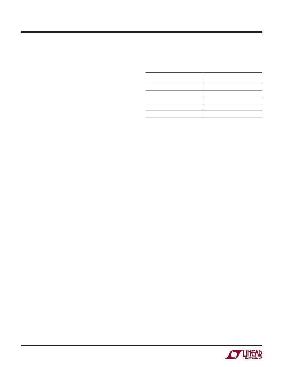
following table demonstrates the effect of the baseline
20nV/√Hz equivalent input control noise from the LTC6412
circuit along with the effect of a higher combined input
noise due to a noisy external control circuit.
CONTROL INPUT TOTAL NOISE
VOLTAGE (nV/√Hz)
PEAK AM NOISE AT 10kHz OFFSET
NEAR MAXIMUM GAIN (dBc/Hz)
20
–142
40
–136
70
–131
100
–128
200
–122
The baseline equivalent 20nV/√Hz input noise is seen to
produce worst-case AM sidebands of –142dBc/Hz which is
near the –147dBm/Hz output noise oor at maximum gain
for a nominal 0dBm output signal. An input control noise
voltage less than 80nV/√Hz is generally recommended to
avoid measurable AM sideband noise. While op amp control
circuit output noise voltage is usually below 80nV/√Hz,
some low power DAC outputs exceed 150nV/√Hz. DACs
with output noise in the range of 100nV/√Hz to 150nV/√Hz
can usually be accommodated with a suitable 2:1 or 3:1
resistor divider network on the DAC output to suppress the
noise amplitude by the same ratio. Noisy DACs in excess
of 150nV/√Hz should be avoided if minimal AM noise is
important in the application.
相关PDF资料 |
PDF描述 |
|---|---|
| LRC-LRF1206LF-01-R025-F | RES .025 OHM 0.5W 1% 1206 SMD |
| LRC-LRF1206LF-01-R010-F | RES .010 OHM 0.5W 1% 1206 SMD |
| AD8221BR-REEL7 | IC AMP INST PREC LN 18MA 8SOIC |
| 170M6411 | FUSE 700A 690V 3BN/50 AR UC |
| MCP601-E/ST | IC OPAMP SNGL 2.7V 8TSSOP |
相关代理商/技术参数 |
参数描述 |
|---|---|
| LTC6412CUFTRPBF | 制造商:LINER 制造商全称:Linear Technology 功能描述:800MHz, 31dB Range Analog-Controlled VGA |
| LTC6412IUF | 制造商:LINER 制造商全称:Linear Technology 功能描述:800MHz, 31dB Range Analog-Controlled VGA |
| LTC6412IUF#PBF | 功能描述:IC VGA ANLG-CNTRL 31DB 24-QFN RoHS:是 类别:集成电路 (IC) >> Linear - Amplifiers - Instrumentation 系列:- 标准包装:150 系列:- 放大器类型:音频 电路数:2 输出类型:- 转换速率:5 V/µs 增益带宽积:12MHz -3db带宽:- 电流 - 输入偏压:100nA 电压 - 输入偏移:500µV 电流 - 电源:6mA 电流 - 输出 / 通道:50mA 电压 - 电源,单路/双路(±):4 V ~ 32 V,±2 V ~ 16 V 工作温度:-40°C ~ 85°C 安装类型:表面贴装 封装/外壳:8-TSSOP(0.173",4.40mm 宽) 供应商设备封装:8-TSSOP 包装:管件 |
| LTC6412IUF#TRPBF | 功能描述:IC VGA ANLG-CNTRL 31DB 24-QFN RoHS:是 类别:集成电路 (IC) >> Linear - Amplifiers - Instrumentation 系列:- 标准包装:150 系列:- 放大器类型:音频 电路数:2 输出类型:- 转换速率:5 V/µs 增益带宽积:12MHz -3db带宽:- 电流 - 输入偏压:100nA 电压 - 输入偏移:500µV 电流 - 电源:6mA 电流 - 输出 / 通道:50mA 电压 - 电源,单路/双路(±):4 V ~ 32 V,±2 V ~ 16 V 工作温度:-40°C ~ 85°C 安装类型:表面贴装 封装/外壳:8-TSSOP(0.173",4.40mm 宽) 供应商设备封装:8-TSSOP 包装:管件 |
| LTC6412IUFPBF | 制造商:LINER 制造商全称:Linear Technology 功能描述:800MHz, 31dB Range Analog-Controlled VGA |
发布紧急采购,3分钟左右您将得到回复。