- 您现在的位置:买卖IC网 > PDF目录5753 > LTC6412IUF#TRPBF (Linear Technology)IC VGA ANLG-CNTRL 31DB 24-QFN PDF资料下载
参数资料
| 型号: | LTC6412IUF#TRPBF |
| 厂商: | Linear Technology |
| 文件页数: | 10/24页 |
| 文件大小: | 0K |
| 描述: | IC VGA ANLG-CNTRL 31DB 24-QFN |
| 标准包装: | 2,500 |
| 放大器类型: | 可变增益 |
| 电路数: | 1 |
| 输出类型: | 差分 |
| -3db带宽: | 800MHz |
| 电流 - 电源: | 110mA |
| 电流 - 输出 / 通道: | 70mA |
| 电压 - 电源,单路/双路(±): | 3 V ~ 3.6 V |
| 工作温度: | -40°C ~ 85°C |
| 安装类型: | 表面贴装 |
| 封装/外壳: | 24-WFQFN 裸露焊盘 |
| 供应商设备封装: | 24-QFN 裸露焊盘(4x4) |
| 包装: | 带卷 (TR) |
LTC6412
18
6412fa
APPLICATIONS INFORMATION
6412 F02
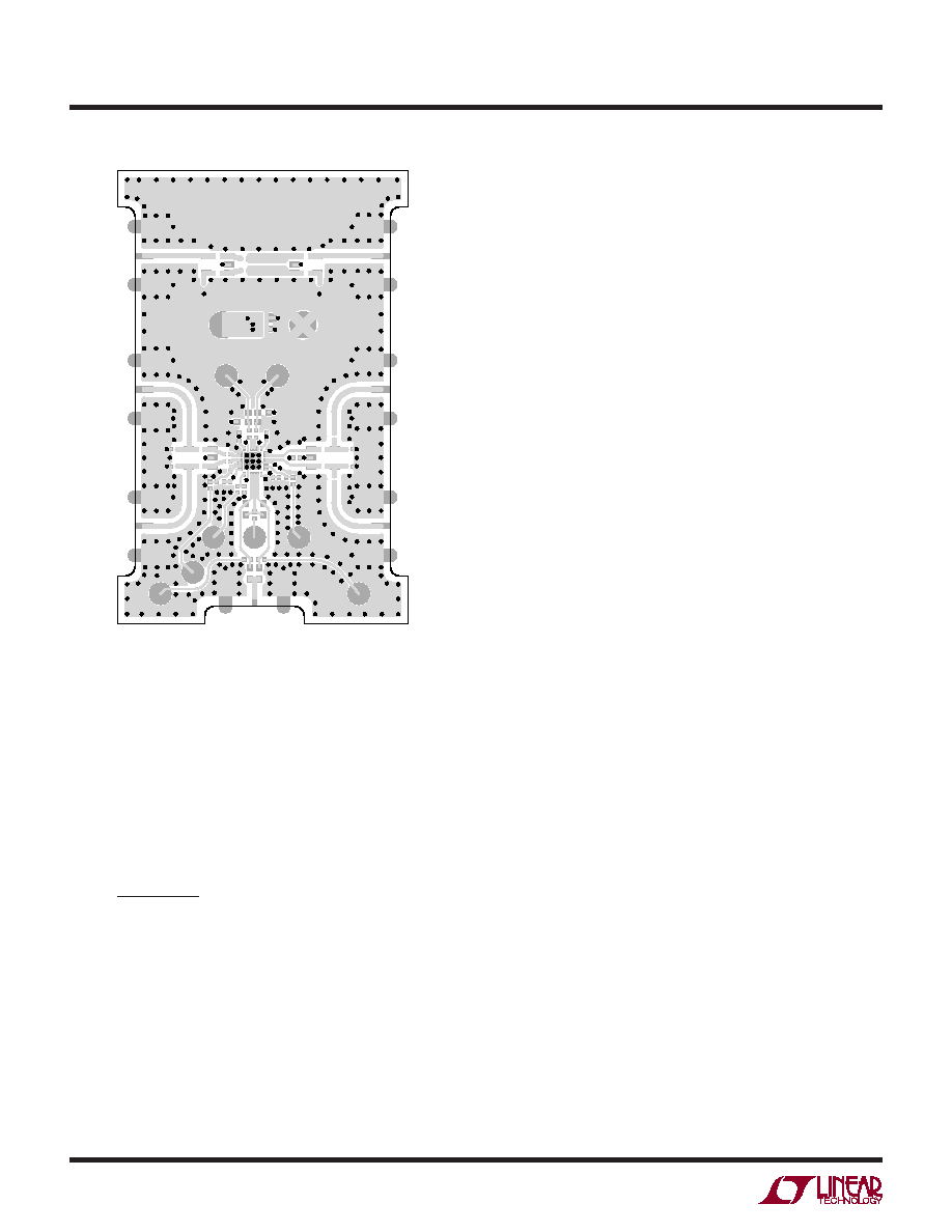
Figure 2. Top Metal for DC1464A. Test Circuit A
Figure 9b shows a further variation of the tuned differential
output where the DC blocking capacitors are brought inside
the tank resonator to participate in the bandpass lter and
transform the VGA output impedance to a lower value.
Here too, the CO capacitor can be split into two separate
shunt capacitors to ground, so any common mode noise
is ltered as well.
Figure 9c shows a ux transformer used to achieve a
50Ω single-ended output. The ux transformer does
not provide the large bandwidth typical of the output
transmission-line transformer shown in Figure 3, but it
usually performs well over smaller bandwidths, especially
when tuned with shunt capacitors (not shown). The ux
transformer design eliminates DC blocking capacitors and
is attractive in rugged applications where the amplier
output is subjected to ESD events and other forms of
transient electrical overstress that do not pass through a
typical RF ux transformer such as the MABAES0061.
Figure 9d shows a discrete LC balun suitable for bandwidths
of approximately 15% to 30%. Larger bandwidths are
difcult to achieve with the number of components shown,
and smaller bandwidths are often limited by component
tolerance effects. Despite these limitations, the discrete
LC balun can be a cost effective output circuit solution.
At resonance, the tuned circuit produces an impedance
transformation along with the differential-to-single-ended
conversion.
DC-Coupled Operation
The LTC6412 is intended for AC-coupled operation. The
translation between the xed input DC common mode
voltage and higher open-collector output DC bias point
makes it impractical to use in DC-coupled applications.
from the output pins should be narrow in keeping with
the high impedance of these terminals; 8 to 10mil trace
width on 1oz copper is a good choice. The 0.1μF capacitors
serve to DC block and decouple as needed. These capacitor
values are adequate down to a few MHz and can be scaled
down for higher application frequencies.
If bandpass ltering is needed at the VGA output of
Figure 9a, then L1 and L2 can be designed to resonate
with a shunt capacitor, CO, at the frequency of interest,
ω =1/√CO(L1 + L2). Alternately, L1 = L2 can be designed
to resonate with two separate capacitors, C1 = C2, so any
common mode noise is ltered as well.
相关PDF资料 |
PDF描述 |
|---|---|
| 0447004.YXP | FUSE 350V MINI T HOLE EBF 4A |
| SL1021B200RS | GAS TUBE GDT 10KA 200V RAD +FS |
| 39711500440 | FUSE 1.5A 125VAC RADIAL SLOW |
| 39711250440 | FUSE 1.25A 125VAC RADIAL SLOW |
| 39711000440 | FUSE 1A 125VAC RADIAL SLOW |
相关代理商/技术参数 |
参数描述 |
|---|---|
| LTC6416 | 制造商:LINER 制造商全称:Linear Technology 功能描述:2 GHz Low Noise Differential 16-Bit ADC Buffer |
| LTC6416CDDB#TRMPBF | 功能描述:IC ADC BUFFER 16BIT DIFF 10-DFN RoHS:是 类别:集成电路 (IC) >> Linear - Amplifiers - Instrumentation 系列:- 标准包装:73 系列:Over-The-Top® 放大器类型:通用 电路数:4 输出类型:满摆幅 转换速率:0.07 V/µs 增益带宽积:200kHz -3db带宽:- 电流 - 输入偏压:1nA 电压 - 输入偏移:285µV 电流 - 电源:50µA 电流 - 输出 / 通道:25mA 电压 - 电源,单路/双路(±):2 V ~ 44 V,±1 V ~ 22 V 工作温度:-40°C ~ 85°C 安装类型:表面贴装 封装/外壳:16-WFDFN 裸露焊盘 供应商设备封装:16-DFN-EP(5x3) 包装:管件 |
| LTC6416CDDB#TRPBF | 功能描述:IC ADC BUFFER 16BIT DIFF 10-DFN RoHS:是 类别:集成电路 (IC) >> Linear - Amplifiers - Instrumentation 系列:- 标准包装:73 系列:Over-The-Top® 放大器类型:通用 电路数:4 输出类型:满摆幅 转换速率:0.07 V/µs 增益带宽积:200kHz -3db带宽:- 电流 - 输入偏压:1nA 电压 - 输入偏移:285µV 电流 - 电源:50µA 电流 - 输出 / 通道:25mA 电压 - 电源,单路/双路(±):2 V ~ 44 V,±1 V ~ 22 V 工作温度:-40°C ~ 85°C 安装类型:表面贴装 封装/外壳:16-WFDFN 裸露焊盘 供应商设备封装:16-DFN-EP(5x3) 包装:管件 |
| LTC6416CDDB-TRMPBF | 制造商:LINER 制造商全称:Linear Technology 功能描述:2 GHz Low Noise Differential 16-Bit ADC Buffer |
| LTC6416CDDB-TRPBF | 制造商:LINER 制造商全称:Linear Technology 功能描述:2 GHz Low Noise Differential 16-Bit ADC Buffer |
发布紧急采购,3分钟左右您将得到回复。