- 您现在的位置:买卖IC网 > PDF目录11029 > LTC6601CUF-1#TRPBF (Linear Technology)IC DRVR FILTER/ADC LN 20-QFN PDF资料下载
参数资料
| 型号: | LTC6601CUF-1#TRPBF |
| 厂商: | Linear Technology |
| 文件页数: | 10/40页 |
| 文件大小: | 0K |
| 描述: | IC DRVR FILTER/ADC LN 20-QFN |
| 标准包装: | 2,500 |
| 频率 - 截止或中心: | 28Mhz |
| 滤波器数: | 3 |
| 滤波器阶数: | 2nd |
| 电源电压: | 2.7 V ~ 5.25 V |
| 安装类型: | 表面贴装 |
| 封装/外壳: | 20-WFQFN 裸露焊盘 |
| 供应商设备封装: | 20-QFN 裸露焊盘(4x4) |
| 包装: | 带卷 (TR) |
第1页第2页第3页第4页第5页第6页第7页第8页第9页当前第10页第11页第12页第13页第14页第15页第16页第17页第18页第19页第20页第21页第22页第23页第24页第25页第26页第27页第28页第29页第30页第31页第32页第33页第34页第35页第36页第37页第38页第39页第40页
LTC6601-1
18
66011f
LTC6601 ideally suited for pre-amplication, level shift-
ing and conversion of single-ended signals to differential
output signals for driving differential input ADCs.
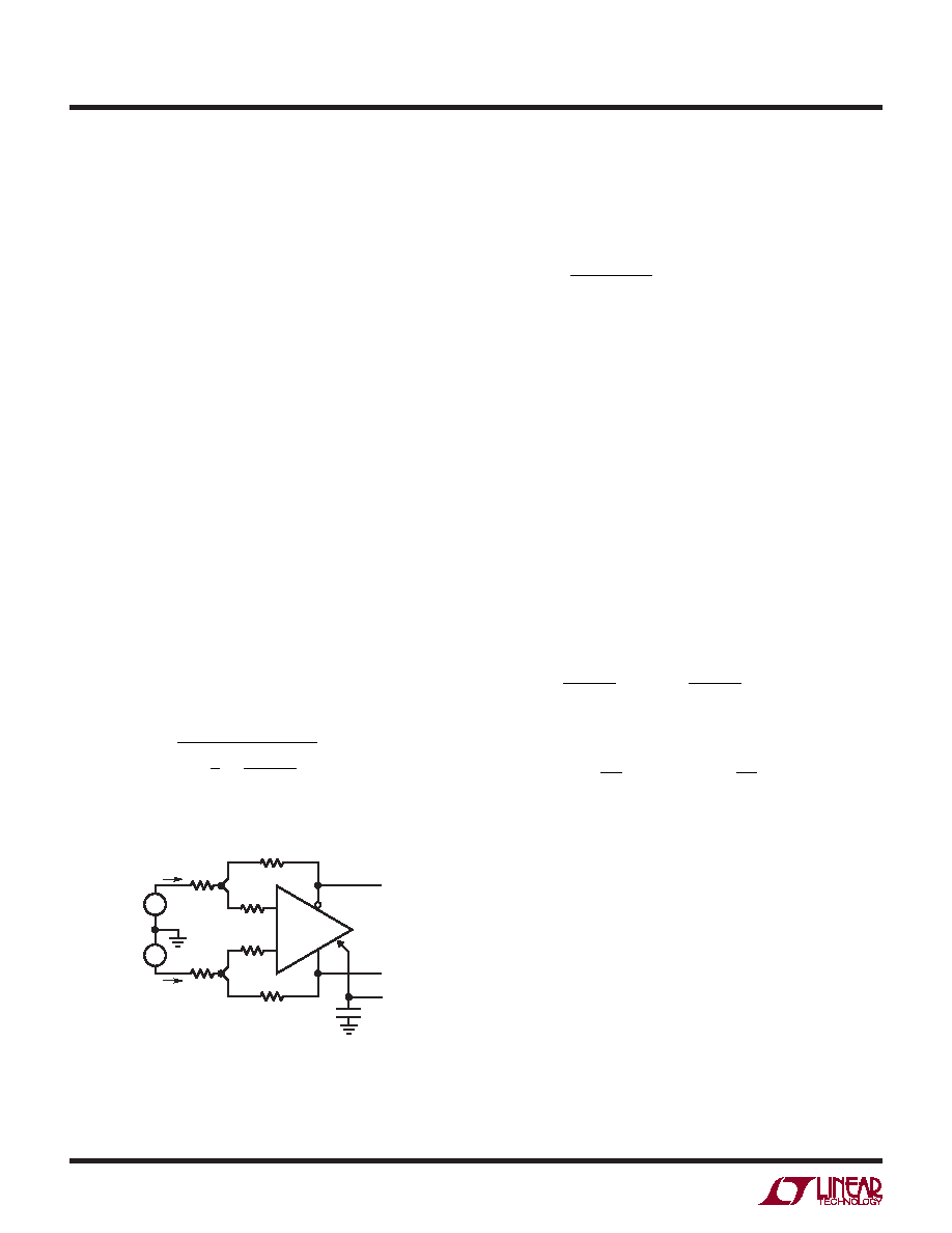
INPUT IMPEDANCE
Calculating the low frequency input impedance of the
LTC6601 depends on how the inputs are driven (whether
they are driven from a single-ended or a differential
source).
Figure 4 shows a simplied low frequency equivalent
circuit of the LTC6601. For balanced input sources (VINP
= –VINM), the low frequency input impedance is given by
the equation:
RINP = RINM = R1
The differential input impedance is simply:
RINDIFF = 2 R1
For single-ended inputs (VINM = 0), the input impedance
actually increases over the balanced differential case due
to the fact the summing node (at the junction of R1, R2
and R3) moves in phase with VINP to bootstrap the input
impedance. Referring to Figure 4 with VINM = 0, the input
impedance looking into either input is:
RINP =RINM
R1
1– 1
2
R2
R1+R2
Input and Output Common Mode Voltage Range
The input common mode voltage is dened as the average
of the two inputs:
VINCM =
VINP + VINM
2
The lower limit of the input common mode range is dic-
tated by the ESD protection diodes at the input. While it
is possible for the inputs to swing below V–, the diodes
will conduct if the inputs are taken a diode drop below V–.
The upper limit of the input common mode range varies
as a function of the lter conguration (GAIN), VOCM po-
tential, and whether or not the inputs are single-ended or
differential. While it is possible to exceed the upper limit
of the common mode range, doing so will degrade lter
linearity. Referring to Figure 4, for linear operation, the
summing junction where R1, R2 and R3 merge together
should be prevented from swinging to within 1.4V of the
V+ power supply.
For the general case, the upper input common mode volt-
age limit should be constrained to:
VOCM
R1
R1+R2
+ VINCM
R2
R1+R2
≤ V+ – 1.4V
Or equivalently:
VINCM ≤ 1+
R1
R2
V+ 1.4V
() R1
R2
VOCM
The specications for input common mode range (VINCMR)
are based on these constraints with R1 = R2 = 100Ω, and
VOCM = mid-supply. Substituting the numbers for a single
3V power supply, (V+ = 3V, V– = 0V) with VOCM =1.5V, and
R1 = R2 = 100Ω, into the above equation, the input com-
mon mode range (VINCMR) is between the two limits:
0V ≤ VINCM ≤ 1.7V
which is as is specied for a 3V supply.
APPLICATIONS INFORMATION
–
+
R2
VOUT
–
VOUT
+
VOCM
VOUTDIFF
0.1μF
66011 F04
R1
RINP
VINP
VINM
R1
R2
R3
+
–
+
–
RINM
Figure 4. Input Impedance
相关PDF资料 |
PDF描述 |
|---|---|
| LTC6601CUF-1#PBF | IC DRVR FILTER/ADC LN 20-QFN |
| LT1568CGN#TRPBF | IC BLOCK BUILD FLTR LONOS 16SSOP |
| LT1568CGN#TR | IC BLOCK BUILD FLTR LONOS 16SSOP |
| LT1568CGN | IC FILTER BUILDING BLOCK 16SSOP |
| LTC1565-31IS8#TRPBF | IC FILTR 7TH ORDER 650KHZ 8-SOIC |
相关代理商/技术参数 |
参数描述 |
|---|---|
| LTC6601CUF-2 | 制造商:LINER 制造商全称:Linear Technology 功能描述:Low Power, Low Distortion, 5MHz to 27MHz, Pin Confi gurable Filter/ADC Driver |
| LTC6601CUF-2#PBF | 功能描述:IC DRVR FILTER/ADC LN 20-QFN RoHS:是 类别:集成电路 (IC) >> 接口 - 滤波器 - 有源 系列:- 产品培训模块:Lead (SnPb) Finish for COTS Obsolescence Mitigation Program 标准包装:1,000 系列:- 滤波器类型:连续时间,带通低通 频率 - 截止或中心:150kHz 滤波器数:4 滤波器阶数:8th 电源电压:4.74 V ~ 11 V,±2.37 V ~ 5.5 V 安装类型:表面贴装 封装/外壳:28-SOIC(0.295",7.50mm 宽) 供应商设备封装:28-SOIC W 包装:带卷 (TR) |
| LTC6601CUF-2#PBF | 制造商:Linear Technology 功能描述:SC-Filters/Active RCLow Power Low Disto |
| LTC6601CUF-2#TRPBF | 功能描述:IC FILTER/ADC DVR LP LD 20-QFN RoHS:是 类别:集成电路 (IC) >> 接口 - 滤波器 - 有源 系列:- 产品培训模块:Lead (SnPb) Finish for COTS Obsolescence Mitigation Program 标准包装:1,000 系列:- 滤波器类型:连续时间,带通低通 频率 - 截止或中心:150kHz 滤波器数:4 滤波器阶数:8th 电源电压:4.74 V ~ 11 V,±2.37 V ~ 5.5 V 安装类型:表面贴装 封装/外壳:28-SOIC(0.295",7.50mm 宽) 供应商设备封装:28-SOIC W 包装:带卷 (TR) |
| LTC6601CUF-2PBF | 制造商:LINER 制造商全称:Linear Technology 功能描述:Low Power, Low Distortion, 5MHz to 27MHz, Pin Confi gurable Filter/ADC Driver |
发布紧急采购,3分钟左右您将得到回复。