- 您现在的位置:买卖IC网 > PDF目录11028 > LTC6601IUF-2#TRPBF (Linear Technology)IC FILTER/ADC DVR LP LD 20-QFN PDF资料下载
参数资料
| 型号: | LTC6601IUF-2#TRPBF |
| 厂商: | Linear Technology |
| 文件页数: | 13/40页 |
| 文件大小: | 0K |
| 描述: | IC FILTER/ADC DVR LP LD 20-QFN |
| 标准包装: | 2,500 |
| 频率 - 截止或中心: | 27MHz |
| 滤波器数: | 3 |
| 滤波器阶数: | 2nd |
| 电源电压: | 2.7 V ~ 5.25 V |
| 安装类型: | 表面贴装 |
| 封装/外壳: | 20-WFQFN 裸露焊盘 |
| 供应商设备封装: | 20-QFN 裸露焊盘(4x4) |
| 包装: | 带卷 (TR) |
第1页第2页第3页第4页第5页第6页第7页第8页第9页第10页第11页第12页当前第13页第14页第15页第16页第17页第18页第19页第20页第21页第22页第23页第24页第25页第26页第27页第28页第29页第30页第31页第32页第33页第34页第35页第36页第37页第38页第39页第40页
LTC6601-2
20
66012f
APPLICATIONS INFORMATION
Table 1 lists the amplier input referred noise for the
LTC6601-2. Tables 2 to10 list the noise referred to the input
pins of the IC for common congurations of the LTC6601-2.
To determine the spot noise at the output, simply multiply
the noise by the Gain = R2/R1. To estimate the integrated
noise at the output, multiply the noise by the gain, and the
square root of the noise bandwidth. The noise bandwidth
depends on the lter conguration. For Figure 2, the noise
bandwidth is 100MHz, or approximately 7 times the lter
bandwidth. Improvements in SNR can be made by adding
an additional RC lter at the output to band limit wide band
noise before feeding ADCs. See the section “Interfacing
the LTC6601 to ADC Converters” for more detail.
Table 1. Amplier (Input Referred) Noise Characteristics for the
LTC6601-2
BIAS PIN PULLED TO V+
BIAS PIN FLOATING
eni
nV/√Hz
in
pA/√Hz
eni
nV/√Hz
in
pA/√Hz
4.7
3
5.2
2.1
LAYOUT CONSIDERATIONS
Because the LTC6601 is a very high speed amplier, it is
sensitive to both stray capacitance and stray inductance.
It is critical that close attention be paid to supply bypass-
ing. For single supply applications, it is recommended
that a high quality 0.1μF surface mount ceramic bypass
capacitor be placed between Pins 14 and 13 with direct
short connections. Pin 13 and the Exposed Pad, Pin 21,
should be tied directly to a low impedance ground plane
with minimal routing. For dual (split) power supplies, it
is recommended that an additional high quality, 0.1μF
ceramic capacitor be used to bypass pin V+ to ground
and V– to ground, again with minimal routing. For driv-
ing large differential loads (<200Ω), additional bypass
capacitance may be needed between V+ and V– for opti-
mal performance. Note that small geometry (e.g., 0603)
surface mount ceramic capacitors have a much higher
self resonant frequency than capacitors with leads, and
perform best in high speed applications.
The VOCM pin should be bypassed to ground with a high
quality ceramic capacitor whose value exceeds 0.01μF,
with direct, short connections. In split supply applications,
the VOCM pin can be either bypassed to ground or directly
hardwired to ground. Be careful not to violate the output
common mode range specications for the VOCM pin.
Stray parasitic capacitances to unused component pins
that set up the lter’s characteristics, should be kept to an
absolute minimum. This prevents deviations from the ideal
frequency response. An ideal layout technique would be to
remove the solder pads for the unused component pins,
and strip away the ground plane underneath these pins to
lower capacitance to an absolute minimum. Floating unused
component pins which set up the lter characteristics will
not reduce the reliability of the LTC6601.
At the output, always keep in mind the differential nature of
the LTC6601, and that it is critical that the load impedances
seen by both outputs (stray or intended), should be as bal-
anced and symmetric as possible. This will help preserve
the natural balance of the LTC6601, which minimizes the
generation of even order harmonics and preserves the
rejection of common mode signals and noise.
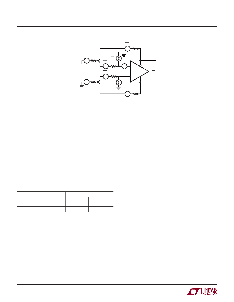
–
+
66012 F05
R1
R3
*
eni2
eno2
enR32
R3
*
enR32
R2
*
enR22
R2
*
enR22
*
enR12
*
enR12
In+2
In–2
Figure 5. Differential Noise Model of the LTC6601
相关PDF资料 |
PDF描述 |
|---|---|
| VE-2TX-IY-F1 | CONVERTER MOD DC/DC 5.2V 50W |
| LTC6601IUF-1#PBF | IC DRVR FILTER/ADC LN 20-QFN |
| VE-2TW-IY-F2 | CONVERTER MOD DC/DC 5.5V 50W |
| VE-2TP-IY-F2 | CONVERTER MOD DC/DC 13.8V 50W |
| LTC1069-1IS8#TRPBF | IC FILTR 8TH ORDER LOWPASS 8SOIC |
相关代理商/技术参数 |
参数描述 |
|---|---|
| LTC6602 | 制造商:LINER 制造商全称:Linear Technology 功能描述:Dual Matched, High Frequency Bandpass/Lowpass Filters |
| LTC6602CUF#PBF | 功能描述:IC FILTER BANDPASS/LOWPASS 24QFN RoHS:是 类别:集成电路 (IC) >> 接口 - 滤波器 - 有源 系列:- 产品培训模块:Lead (SnPb) Finish for COTS Obsolescence Mitigation Program 标准包装:1,000 系列:- 滤波器类型:连续时间,带通低通 频率 - 截止或中心:150kHz 滤波器数:4 滤波器阶数:8th 电源电压:4.74 V ~ 11 V,±2.37 V ~ 5.5 V 安装类型:表面贴装 封装/外壳:28-SOIC(0.295",7.50mm 宽) 供应商设备封装:28-SOIC W 包装:带卷 (TR) |
| LTC6602CUF#TRPBF | 功能描述:IC FILTER BANDPASS/LOWPASS 24QFN RoHS:是 类别:集成电路 (IC) >> 接口 - 滤波器 - 有源 系列:- 产品培训模块:Lead (SnPb) Finish for COTS Obsolescence Mitigation Program 标准包装:1,000 系列:- 滤波器类型:连续时间,带通低通 频率 - 截止或中心:150kHz 滤波器数:4 滤波器阶数:8th 电源电压:4.74 V ~ 11 V,±2.37 V ~ 5.5 V 安装类型:表面贴装 封装/外壳:28-SOIC(0.295",7.50mm 宽) 供应商设备封装:28-SOIC W 包装:带卷 (TR) |
| LTC6602CUF-PBF | 制造商:LINER 制造商全称:Linear Technology 功能描述:Dual Matched, High Frequency Bandpass/Lowpass Filters |
| LTC6602CUF-TRPBF | 制造商:LINER 制造商全称:Linear Technology 功能描述:Dual Matched, High Frequency Bandpass/Lowpass Filters |
发布紧急采购,3分钟左右您将得到回复。