参数资料
| 型号: | LTC6909IMS#PBF |
| 厂商: | Linear Technology |
| 文件页数: | 4/22页 |
| 文件大小: | 0K |
| 描述: | IC OSC SILICON 6.67MHZ 16-MSOP |
| 产品目录绘图: | 16-MSOP |
| 标准包装: | 37 |
| 类型: | 振荡器 - 硅 |
| 频率: | 12.5kHz ~ 6.67MHz |
| 电源电压: | 2.7 V ~ 5.5 V |
| 电流 - 电源: | 2.4mA |
| 工作温度: | -40°C ~ 85°C |
| 封装/外壳: | 16-TFSOP(0.118",3.00mm 宽) |
| 包装: | 管件 |
| 供应商设备封装: | 16-MSOP |
| 安装类型: | 表面贴装 |
| 产品目录页面: | 1715 (CN2011-ZH PDF) |
LTC6909
12
6909fa
SELECTING THE FREqUENCY-SETTING RESISTOR
The LTC6909 has a master oscillator frequency range
spanning 100kHz to 20MHz depending on the RSET resis-
tor value. However, accuracy may suffer if the oscillator
is operated at a master oscillator frequency greater than
10MHz with a supply voltage lower than 4V. With a linear
correspondence between the master oscillator period and
the RSET resistance, a simple equation relates resistance
with frequency.
RSET =10k 20MHz/fMASTER
RSETMIN = 10k (5V supply), 20k (2.7V supply),
RSETMAX = 2M
Any RSET resistor tolerance will shift the output frequency
by the same amount.
ALTERNATIVE METHODS OF SETTING THE OUTPUT
FREqUENCY OF THE LTC6909
The oscillator may be programmed by any method that
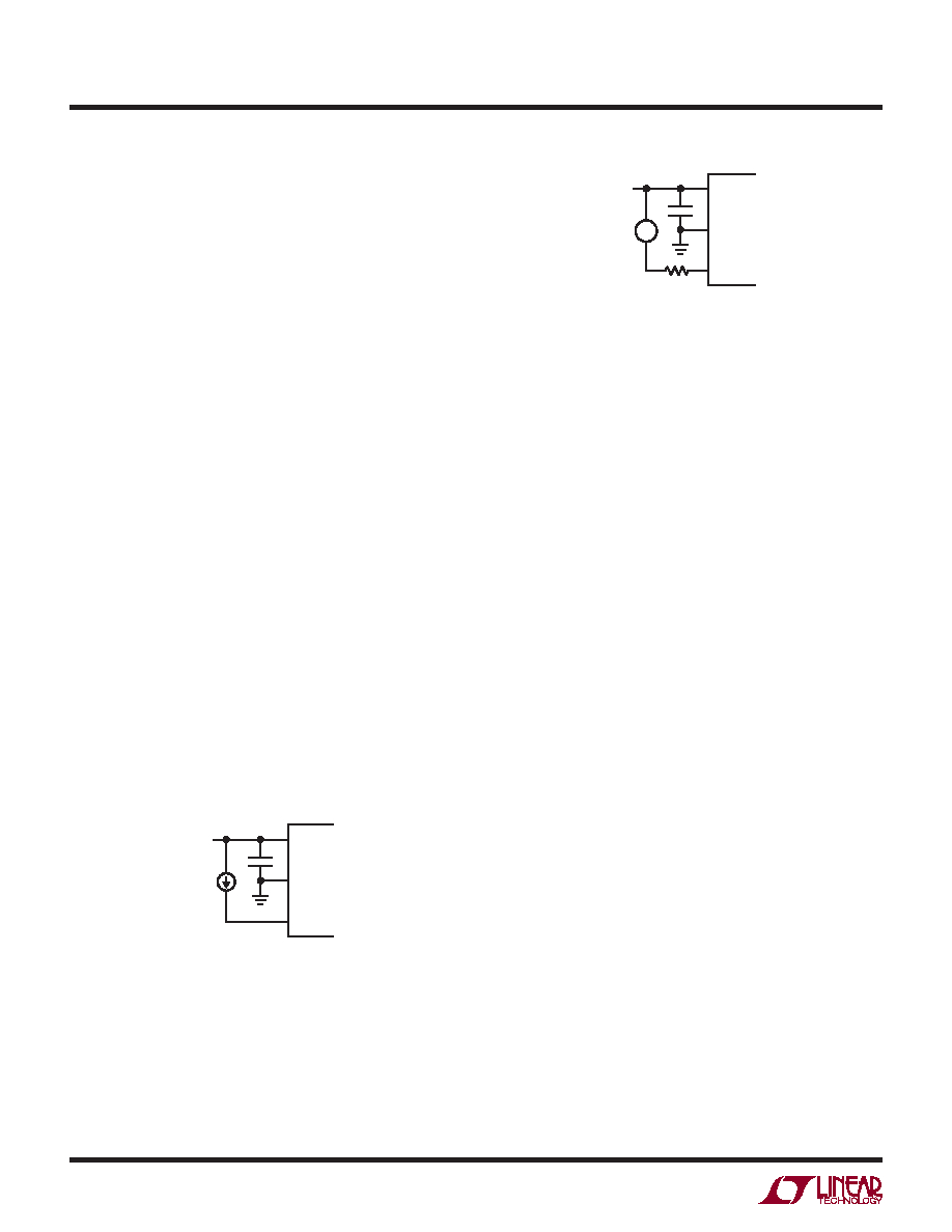
sources a current into the SET pin. The circuit in Figure 4
setstheoscillatorfrequencyusingaprogrammablecurrent
source and in the expression for fOUT, the resistor RSET is
replacedbytheratioof1.1V/ICONTROL.Asalreadyexplained
in the Operation section, the voltage difference between
V+ and SET is approximately 1.1V ±5%, therefore, the
Figure 4 circuit is less accurate than if a resistor controls
the output frequency.
Figure 4. Current Controlled Oscillator
Figure 5 shows the LTC6909 configured as a VCO. A volt-
age source is connected in series with an external 10k
resistor. The master oscillator frequency, fMASTER, will
vary with VCONTROL, that is the voltage source connected
between V+ and the SET pin. Again, this circuit decouples
Figure 5. Voltage Controlled Oscillator
the relationship between the input current and the volt-
age between V+ and SET; the frequency accuracy will be
degraded. The oscillator frequency, however, will increase
monotonically with decreasing VCONTROL.
SETTING THE MODULATION RATE OF THE LTC6909
The modulation rate of the LTC6909 is equal to fOUT/N,
where N is the modulation rate divider setting, which is
determinedbythestateoftheMODpin.TheMODpinshould
be tied to ground for the N = 16 setting. Floating the MOD
pin selects N = 32. The MOD pin should be tied to V+ for
the N = 64 setting. To disable the SSFM, connect one of
the active outputs to the MOD pin. An AC detector circuit
shuts down the modulation circuitry if a frequency that is
close to the output frequency is detected at the MOD pin.
When the MOD pin is floated, for the fOUT/32 modulation
rate, it must be bypassed by at least a 1nF capacitor
to GND. Any AC signal coupling to the MOD pin could
potentiallybedetectedandstopthefrequencymodulation.
DRIVING LOGIC CIRCUITS
The outputs of the LTC6909 are suitable for driving gen-
eral digital logic circuits. However, the form of frequency
spreading used in the LTC6909 may not be suitable for
many logic designs. Many logic designs have fairly tight
timing and cycle-to-cycle jitter requirements. These sys-
temsoftenbenefitfromaspreadspectrumclockingsystem
where the frequency is slowly and linearly modulated by a
triangularwaveform,notapseudorandomwaveform.This
typeoffrequencyspreadingmaintainsaminimaldifference
in the timing from one clock edge to the next adjacent
clock edge (cycle-to-cycle jitter). The LTC6909 uses a
pseudorandom modulating signal where the frequency
CBYP
ICONTROL
fMASTER = 10k (20MHz/1.13V) ICONTROL(A)
V+A
V+
GND
SET
6909 F04
CBYP
VCONTROL
fOUT = 10k 20MHz/RSET(1 – VCONTROL/1.13V)
V+A
V+
GND
SET
6909 F05
RSET
+–
ApplicAtions inForMAtion
相关PDF资料 |
PDF描述 |
|---|---|
| VE-B4P-IU-S | CONVERTER MOD DC/DC 13.8V 200W |
| VE-B4N-IU-S | CONVERTER MOD DC/DC 18.5V 200W |
| LTC6902IMS#PBF | IC OSC SILICON 20MHZ 10MSOP |
| VE-B4M-IU-S | CONVERTER MOD DC/DC 10V 200W |
| LTC6992HS6-3#TRMPBF | IC OSC SILICON 1MHZ TSOT23-6 |
相关代理商/技术参数 |
参数描述 |
|---|---|
| LTC6909IMS-TRPBF | 制造商:LINER 制造商全称:Linear Technology 功能描述:1 to 8 Output, Multiphase Silicon Oscillator with Spread Spectrum Modulation |
| LTC690C | 制造商:LINER 制造商全称:Linear Technology 功能描述:Microprocessor Supervisory Circuits |
| LTC690CN8 | 功能描述:IC MPU SUPERVISORY CIRCUIT 8-DIP RoHS:否 类别:集成电路 (IC) >> PMIC - 监控器 系列:- 标准包装:1 系列:- 类型:简单复位/加电复位 监视电压数目:1 输出:开路漏极或开路集电极 复位:高有效 复位超时:- 电压 - 阀值:1.8V 工作温度:-40°C ~ 125°C 安装类型:表面贴装 封装/外壳:6-TSOP(0.059",1.50mm 宽)5 引线 供应商设备封装:5-TSOP 包装:剪切带 (CT) 其它名称:NCP301HSN18T1GOSCT |
| LTC690CN8#PBF | 功能描述:IC MPU SUPERVISORY CIRCUIT 8-DIP RoHS:是 类别:集成电路 (IC) >> PMIC - 监控器 系列:- 其它有关文件:STM6905 View All Specifications 标准包装:1 系列:- 类型:多压监控器 监视电压数目:5 输出:开路漏极或开路集电极 复位:低有效 复位超时:最小为 140 ms 电压 - 阀值:2.188V,2.955V,可调,可调,可调 工作温度:-40°C ~ 85°C 安装类型:表面贴装 封装/外壳:8-TSSOP,8-MSOP(0.118",3.00mm 宽) 供应商设备封装:8-TSSOP 包装:Digi-Reel® 产品目录页面:1197 (CN2011-ZH PDF) 其它名称:497-8728-6 |
| LTC690CN8PBF | 制造商:LINER 制造商全称:Linear Technology 功能描述:Microprocessor Supervisory Circuits |
发布紧急采购,3分钟左右您将得到回复。