- 您现在的位置:买卖IC网 > PDF目录5375 > LTC6910-1CTS8#TRPBF (Linear Technology)IC PGA DIGITAL R-R I/O TSOT23-8 PDF资料下载
参数资料
| 型号: | LTC6910-1CTS8#TRPBF |
| 厂商: | Linear Technology |
| 文件页数: | 7/24页 |
| 文件大小: | 0K |
| 描述: | IC PGA DIGITAL R-R I/O TSOT23-8 |
| 标准包装: | 2,500 |
| 放大器类型: | 可编程增益 |
| 电路数: | 1 |
| 输出类型: | 满摆幅 |
| 转换速率: | 16 V/µs |
| 增益带宽积: | 11MHz |
| 电压 - 输入偏移: | 1500µV |
| 电流 - 电源: | 3.5mA |
| 电流 - 输出 / 通道: | 35mA |
| 电压 - 电源,单路/双路(±): | 2.7 V ~ 10.5 V,±2.7 V ~ 5.25 V |
| 工作温度: | 0°C ~ 70°C |
| 安装类型: | 表面贴装 |
| 封装/外壳: | SOT-23-8 薄型,TSOT-23-8 |
| 供应商设备封装: | TSOT-23-8 |
| 包装: | 带卷 (TR) |
LTC6910-1
LTC6910-2/LTC6910-3
15
6910123fa
–
+
INPUT R ARRAY
FEEDBACK R ARRAY
V–
6910 F04
OUT
V+
10k
MOS-INPUT
OP AMP
IN
AGND
10k
2
V–
4
V+
8
G1
G2
G0
1
3
CMOS LOGIC
6
7
5
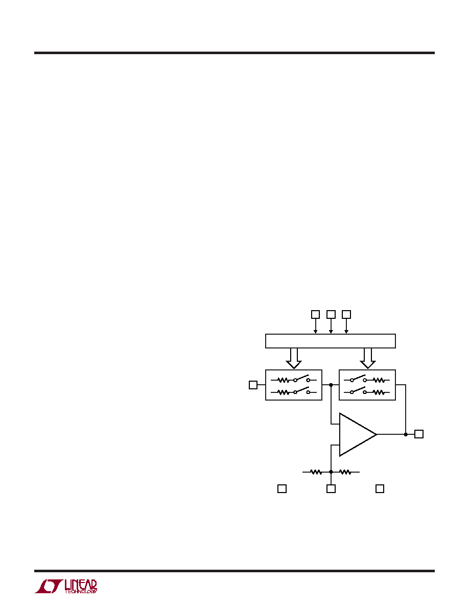
Figure 4. Block Diagram
UU
U
PI FU CTIO S
Where AGND does not connect to a ground plane, as in
Figures 1 and 3, it is important to AC-bypass the AGND pin.
This is especially true when AGND is used as a reference
voltage for other circuitry. Also, without a bypass capaci-
tor, wideband noise will enter the signal path from the
internal voltage divider resistors that set the DC voltage on
AGND. This noise can reduce SNR by 3dB at high gain
settings. The resistors present a Thévenin equivalent of
approximately 5k to the AGND pin. An external capacitor
from AGND to the ground plane, whose impedance is well
below 5k at frequencies of interest, will suppress this
noise. A 1
Fhighqualitycapacitoriseffectiveinsuppress-
ing resistor noise for frequencies down to 1kHz. Larger
capacitors extend this suppression to proportionately
lower frequencies. This issue does not arise in symmetri-
cal dual supply applications (Figure 2) because AGND
goes directly to ground.
In applications requiring an analog ground reference other
than halfway between the supply rails, the user can over-
ride the built-in analog ground reference by tying the
AGND pin to a reference voltage within the AGND voltage
range specified in the Electrical Characteristics table. The
AGND pin will load the external reference with approxi-
mately 5k returned to the mid-supply potential. AGND
should still be capacitively bypassed to a ground plane as
noted above. Do not connect the AGND pin to the V– pin.
IN (Pin 3): Analog Input. The input signal to the amplifier
in the LTC6910-X is the voltage difference between the IN
and AGND pins. The IN pin connects internally to a digitally
controlled resistance whose other end is a current sum-
ming point at the same potential as the AGND pin (Fig-
ure 4). At unity gain (digital input 001), the value of this
input resistance is approximately 10k
and the IN voltage
range is rail-to-rail (V+ to V–). At gain settings above unity
(digital input 010 or higher), the input resistance falls.
Also, the linear input voltage range falls in inverse propor-
tion to gain. (The higher gains are designed to boost lower
level signals with good noise performance.) Tables 1, 2,
and 3 summarize this behavior. In the “zero” gain state
(digital input 000), analog switches disconnect the IN pin
internally and this pin presents a very high input resis-
tance. The input may vary from rail to rail in the “zero” gain
setting but the output is insensitive to it and remains at the
AGND potential. Circuitry driving the IN pin must consider
the LTC6910-X’s input resistance and the variation of this
resistance when used at multiple gain settings. Signal
sources with significant output resistance may introduce
a gain error as the source’s output resistance and the
LTC6910-X’s input resistance form a voltage divider. This
is especially true at the higher gain settings where the
input resistance is lowest.
In single supply voltage applications at elevated gain
settings (digital input 010 or higher), it is important to
remember that the LTC6910-X’s DC ground reference for
both input and output is AGND, not V–. With increasing
gains, the LTC6910-X’s input voltage range for unclipped
output is no longer rail-to-rail but shrinks toward AGND.
The OUT pin also swings positive or negative with respect
to AGND. At unity gain (digital input 001), both IN and OUT
voltages can swing from rail to rail (Tables 1, 2, 3).
相关PDF资料 |
PDF描述 |
|---|---|
| 1-535541-0 | CONN RECEPT 12POS .100 VERT AU |
| MMH21-014 | CONN RACK/PANEL 14POS 5A |
| MMK23-0141A1 | CONN RACK/PANEL 14POS 5A |
| CS3013-FNZ | IC OP AMP LOW NOISE/PWR 8-QFN |
| MV10-516R/SX-BOTTLE | CONN RING VINYL INSUL #5/16 50PC |
相关代理商/技术参数 |
参数描述 |
|---|---|
| LTC6910-1HTS8 | 制造商:LINER 制造商全称:Linear Technology 功能描述:Digitally Controlled Programmable Gain Amplifiers in SOT-23 |
| LTC6910-1HTS8#TR | 功能描述:IC PGA DIGITAL R-R OUT TSOT23-8 RoHS:否 类别:集成电路 (IC) >> Linear - Amplifiers - Instrumentation 系列:- 标准包装:1,000 系列:- 放大器类型:电压反馈 电路数:4 输出类型:满摆幅 转换速率:33 V/µs 增益带宽积:20MHz -3db带宽:30MHz 电流 - 输入偏压:2nA 电压 - 输入偏移:3000µV 电流 - 电源:2.5mA 电流 - 输出 / 通道:30mA 电压 - 电源,单路/双路(±):4.5 V ~ 16.5 V,±2.25 V ~ 8.25 V 工作温度:-40°C ~ 85°C 安装类型:表面贴装 封装/外壳:14-SOIC(0.154",3.90mm 宽) 供应商设备封装:14-SOIC 包装:带卷 (TR) |
| LTC6910-1HTS8#TRM | 功能描述:IC PGA DIGITAL R-R OUT TSOT23-8 RoHS:否 类别:集成电路 (IC) >> Linear - Amplifiers - Instrumentation 系列:- 标准包装:1,000 系列:- 放大器类型:电压反馈 电路数:4 输出类型:满摆幅 转换速率:33 V/µs 增益带宽积:20MHz -3db带宽:30MHz 电流 - 输入偏压:2nA 电压 - 输入偏移:3000µV 电流 - 电源:2.5mA 电流 - 输出 / 通道:30mA 电压 - 电源,单路/双路(±):4.5 V ~ 16.5 V,±2.25 V ~ 8.25 V 工作温度:-40°C ~ 85°C 安装类型:表面贴装 封装/外壳:14-SOIC(0.154",3.90mm 宽) 供应商设备封装:14-SOIC 包装:带卷 (TR) |
| LTC6910-1HTS8#TRMPBF | 功能描述:IC PGA DIGITAL R-R I/O TSOT23-8 RoHS:是 类别:集成电路 (IC) >> Linear - Amplifiers - Instrumentation 系列:- 标准包装:2,500 系列:- 放大器类型:通用 电路数:1 输出类型:满摆幅 转换速率:0.11 V/µs 增益带宽积:350kHz -3db带宽:- 电流 - 输入偏压:4nA 电压 - 输入偏移:20µV 电流 - 电源:260µA 电流 - 输出 / 通道:20mA 电压 - 电源,单路/双路(±):2.7 V ~ 36 V,±1.35 V ~ 18 V 工作温度:-40°C ~ 85°C 安装类型:表面贴装 封装/外壳:8-SOIC(0.154",3.90mm 宽) 供应商设备封装:8-SO 包装:带卷 (TR) |
| LTC6910-1HTS8#TRPBF | 功能描述:IC PGA DIGITAL R-R I/O TSOT23-8 RoHS:是 类别:集成电路 (IC) >> Linear - Amplifiers - Instrumentation 系列:- 标准包装:2,500 系列:- 放大器类型:通用 电路数:1 输出类型:满摆幅 转换速率:0.11 V/µs 增益带宽积:350kHz -3db带宽:- 电流 - 输入偏压:4nA 电压 - 输入偏移:20µV 电流 - 电源:260µA 电流 - 输出 / 通道:20mA 电压 - 电源,单路/双路(±):2.7 V ~ 36 V,±1.35 V ~ 18 V 工作温度:-40°C ~ 85°C 安装类型:表面贴装 封装/外壳:8-SOIC(0.154",3.90mm 宽) 供应商设备封装:8-SO 包装:带卷 (TR) |
发布紧急采购,3分钟左右您将得到回复。