- 您现在的位置:买卖IC网 > PDF目录5375 > LTC6910-3CTS8#TR (Linear Technology)IC PGA DIGITAL R-R OUT TSOT23-8 PDF资料下载
参数资料
| 型号: | LTC6910-3CTS8#TR |
| 厂商: | Linear Technology |
| 文件页数: | 6/24页 |
| 文件大小: | 0K |
| 描述: | IC PGA DIGITAL R-R OUT TSOT23-8 |
| 标准包装: | 2,500 |
| 放大器类型: | 可编程增益 |
| 电路数: | 1 |
| 输出类型: | 满摆幅 |
| 转换速率: | 16 V/µs |
| 增益带宽积: | 11MHz |
| 电压 - 输入偏移: | 1500µV |
| 电流 - 电源: | 3.5mA |
| 电流 - 输出 / 通道: | 35mA |
| 电压 - 电源,单路/双路(±): | 2.7 V ~ 10.5 V,±2.7 V ~ 5.25 V |
| 工作温度: | 0°C ~ 70°C |
| 安装类型: | 表面贴装 |
| 封装/外壳: | SOT-23-8 薄型,TSOT-23-8 |
| 供应商设备封装: | TSOT-23-8 |
| 包装: | 带卷 (TR) |
LTC6910-1
LTC6910-2/LTC6910-3
14
6910123fa
OUT (Pin 1): Analog Output. This is the output of an
internal operational amplifier and swings to near the
power supply rails (V+ and V–) as specified in the Electrical
Characteristics table. The internal op amp remains active
at all times, including the zero gain setting (digital input
000). As with other amplifier circuits, loading the output as
lightly as possible will minimize signal distortion and gain
error. The Electrical Characteristics table shows perfor-
mance at output currents up to 10mA and current limits
that occur when the output is shorted to midsupply at 2.7V
and
±5V supplies. Signal outputs above 10mA are pos-
sible but current-limiting circuitry will begin to affect
amplifier performance at approximately 20mA. Long-term
operation above 20mA output is not recommended. Do
not exceed maximum junction temperature of 150
°C. The
output will drive capacitive loads up to 50pF. Capacitances
higher than 50pF should be isolated by a series resistor to
preserve AC stability.
AGND (Pin 2): Analog Ground. The AGND pin is at the
midpoint of an internal resistive voltage divider, develop-
ing a potential halfway between the V+ and V– pins, with an
equivalent series resistance to the pin of nominally 5k
(Figure 4). AGND is also the noninverting input of the
internal op amp, which makes it the ground reference
voltage for the IN and OUT pins. Because of this, very
“clean” grounding is important, including an analog ground
plane surrounding the package.
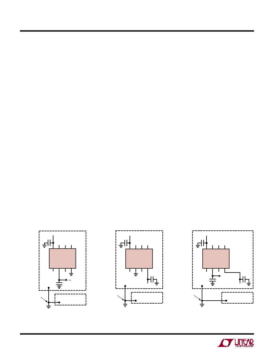
Recommended analog ground plane connection depends
on how power is applied to the LTC6910-X (Figures 1, 2,
and 3). Single power supply applications typically use V–
for the system signal ground. The analog ground plane in
single-supply applications should therefore tie to V–, and
the AGND pin should be bypassed to this ground plane by
a high quality capacitor of at least 1
F (Figure 1). The
AGND pin then provides an internal analog reference
voltage at half the supply voltage (with internal resistance
of approximately 5k
) which is the center of the swing
range for both input and output. Dual supply applications
with symmetrical supplies (such as
±5V) have a natural
system ground at zero volts, which can drive the analog
ground plane; AGND then connects directly to the ground
plane, making zero volts the input and output reference
voltage for the LTC6910-X (Figure 2). Finally, if a dual
power supply is asymmetrical, the supply ground is still
the natural ground plane voltage. To maximize signal
swing capability with an asymmetrical supply, however, it
is often desirable to refer the LTC6910-X’s analog input
and output to a voltage equidistant from the two supply
rails V+ and V–. The AGND pin will provide such a potential
when open-circuited and bypassed with a capacitor (Fig-
ure 3), just as with a single power supply, but now the
ground plane connection is different and the LTC6910-X’s
V+ and V– pins are both isolated from this ground plane.
UU
U
PI FU CTIO S
LTC6910-X
DIGITAL GROUND PLANE
(IF ANY)
ANALOG
GROUND
PLANE
1
SINGLE-POINT
SYSTEM GROUND
23
4
REFERENCE
V+
2
6910 F01
876
5
0.1
F
V+
1
F
LTC6910-X
DIGITAL GROUND PLANE
(IF ANY)
ANALOG
GROUND
PLANE
1
SINGLE-POINT
SYSTEM GROUND
23
4
6910 F02
876
5
0.1
F
V+
0.1
F
V–
Figure 2. Symmetrical Dual Supply
Ground Plane Connection
Figure 1. Single Supply
Ground Plane Connection
LTC6910-X
DIGITAL GROUND PLANE
(IF ANY)
ANALOG
GROUND
PLANE
1
SINGLE-POINT
SYSTEM GROUND
23
4
6910 F03
876
5
0.1
F
V+
0.1
F
1
F
V–
MID-SUPPLY
REFERENCE
Figure 3. Asymmetrical Dual
Supply Ground Plane Connection
相关PDF资料 |
PDF描述 |
|---|---|
| LTC6910-1CTS8#TR | IC PGA DIGITAL R-R OUT TSOT23-8 |
| MME25-011 | CONN RACK/PANEL 11POS 5A |
| 5535512-2 | CONN RECEPT 20POS .100 RT/A DUAL |
| LTC6910-2CTS8#TR | IC PGA DIGITAL R-R OUT TSOT23-8 |
| OP1177ARMZ | IC OPAMP GP 1.3MHZ PREC LN 8MSOP |
相关代理商/技术参数 |
参数描述 |
|---|---|
| LTC6910-3HTS8 | 制造商:LINER 制造商全称:Linear Technology 功能描述:Digitally Controlled Programmable Gain Amplifiers in SOT-23 |
| LTC6910-3HTS8#TR | 功能描述:IC PGA DIGITAL R-R OUT TSOT23-8 RoHS:否 类别:集成电路 (IC) >> Linear - Amplifiers - Instrumentation 系列:- 标准包装:1,000 系列:- 放大器类型:电压反馈 电路数:4 输出类型:满摆幅 转换速率:33 V/µs 增益带宽积:20MHz -3db带宽:30MHz 电流 - 输入偏压:2nA 电压 - 输入偏移:3000µV 电流 - 电源:2.5mA 电流 - 输出 / 通道:30mA 电压 - 电源,单路/双路(±):4.5 V ~ 16.5 V,±2.25 V ~ 8.25 V 工作温度:-40°C ~ 85°C 安装类型:表面贴装 封装/外壳:14-SOIC(0.154",3.90mm 宽) 供应商设备封装:14-SOIC 包装:带卷 (TR) |
| LTC6910-3HTS8#TRM | 功能描述:IC PGA DIGITAL R-R OUT TSOT23-8 RoHS:否 类别:集成电路 (IC) >> Linear - Amplifiers - Instrumentation 系列:- 标准包装:1,000 系列:- 放大器类型:电压反馈 电路数:4 输出类型:满摆幅 转换速率:33 V/µs 增益带宽积:20MHz -3db带宽:30MHz 电流 - 输入偏压:2nA 电压 - 输入偏移:3000µV 电流 - 电源:2.5mA 电流 - 输出 / 通道:30mA 电压 - 电源,单路/双路(±):4.5 V ~ 16.5 V,±2.25 V ~ 8.25 V 工作温度:-40°C ~ 85°C 安装类型:表面贴装 封装/外壳:14-SOIC(0.154",3.90mm 宽) 供应商设备封装:14-SOIC 包装:带卷 (TR) |
| LTC6910-3HTS8#TRMPBF | 功能描述:IC PGA DIGITAL R-R I/O TSOT23-8 RoHS:是 类别:集成电路 (IC) >> Linear - Amplifiers - Instrumentation 系列:- 标准包装:1,000 系列:- 放大器类型:电压反馈 电路数:4 输出类型:满摆幅 转换速率:33 V/µs 增益带宽积:20MHz -3db带宽:30MHz 电流 - 输入偏压:2nA 电压 - 输入偏移:3000µV 电流 - 电源:2.5mA 电流 - 输出 / 通道:30mA 电压 - 电源,单路/双路(±):4.5 V ~ 16.5 V,±2.25 V ~ 8.25 V 工作温度:-40°C ~ 85°C 安装类型:表面贴装 封装/外壳:14-SOIC(0.154",3.90mm 宽) 供应商设备封装:14-SOIC 包装:带卷 (TR) |
| LTC6910-3HTS8#TRPBF | 功能描述:IC PGA DIGITAL R-R I/O TSOT23-8 RoHS:是 类别:集成电路 (IC) >> Linear - Amplifiers - Instrumentation 系列:- 标准包装:2,500 系列:- 放大器类型:通用 电路数:1 输出类型:满摆幅 转换速率:0.11 V/µs 增益带宽积:350kHz -3db带宽:- 电流 - 输入偏压:4nA 电压 - 输入偏移:20µV 电流 - 电源:260µA 电流 - 输出 / 通道:20mA 电压 - 电源,单路/双路(±):2.7 V ~ 36 V,±1.35 V ~ 18 V 工作温度:-40°C ~ 85°C 安装类型:表面贴装 封装/外壳:8-SOIC(0.154",3.90mm 宽) 供应商设备封装:8-SO 包装:带卷 (TR) |
发布紧急采购,3分钟左右您将得到回复。