- 您现在的位置:买卖IC网 > PDF目录3298 > LTC6911IMS-2#TRPBF (Linear Technology)IC PGA DIGITAL R-R DUAL 10MSOP PDF资料下载
参数资料
| 型号: | LTC6911IMS-2#TRPBF |
| 厂商: | Linear Technology |
| 文件页数: | 4/20页 |
| 文件大小: | 0K |
| 描述: | IC PGA DIGITAL R-R DUAL 10MSOP |
| 标准包装: | 2,500 |
| 放大器类型: | 可编程增益 |
| 电路数: | 2 |
| 输出类型: | 满摆幅 |
| 转换速率: | 16 V/µs |
| 增益带宽积: | 11MHz |
| 电压 - 输入偏移: | 2000µV |
| 电流 - 电源: | 3.1mA |
| 电流 - 输出 / 通道: | 35mA |
| 电压 - 电源,单路/双路(±): | 2.7 V ~ 10.5 V,±2.7 V ~ 5.25 V |
| 工作温度: | -40°C ~ 85°C |
| 安装类型: | 表面贴装 |
| 封装/外壳: | 10-TFSOP,10-MSOP(0.118",3.00mm 宽) |
| 供应商设备封装: | 10-MSOP |
| 包装: | 带卷 (TR) |
LTC6911-1/LTC6911-2
12
sn691112 691112fs
UU
U
PI FU CTIO S
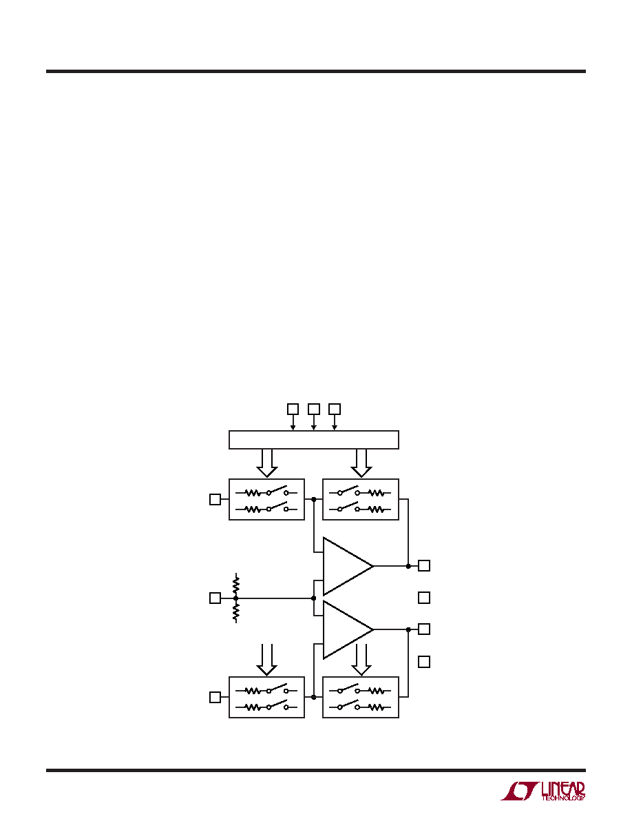
INA (Pin 1): Analog Input. The input signal to the A channel
amplifier of the LTC6911-X is the voltage difference be-
tween the INA and AGND pin. The INA pin connects
internally to a digitally controlled resistance whose other
end is a current summing point at the same potential as the
AGND pin (Figure 1). At unity gain (digital input 001), the
value of this input resistance is approximately 10k
and
the INA pin voltage range is rail-to-rail (V+ to V–). At gain
settings above unity, the input resistance falls. The linear
input range at INA also falls inversely proportional to the
programmed gain. Tables 1 and 2 summarize this behav-
ior. The higher gains are designed to boost lower level
signals with good noise performance. In the “zero” gain
state (digital input 000), analog switches disconnect the
INA pin internally and this pin presents a very high input
resistance. The input may vary from rail to rail in the “zero”
gain setting, but the output is insensitive to it and is forced
to the AGND potential.
Circuitry driving the INA pin must consider the LTC6911-X’s
input resistance, its lot-to-lot variance, and the variation of
this resistance from gain setting to gain setting. Signal
sources with significant output resistance may introduce
a gain error as the source’s output resistance and the
LTC6911-X’s input resistance form a voltage divider. This
is especially true at higher gain settings where the input
resistance is the lowest.
In single supply voltage applications, it is important to
remember that the LTC6911-X’s DC ground reference for
both input and output is AGND, not V–. With increasing
gains, the LTC6911-X’s input voltage range for an unclipped
output is no longer rail-to-rail but diminishes inversely to
gain, centered about the AGND potential.
Figure 1. Block Diagram
–
+
INPUT R ARRAY
FEEDBACK R ARRAY
OUTA
MOS-INPUT
OP AMP
MOS-INPUT
OP AMP
INA
G1
G2
G0
10
V–
9
V+
691112 F01
7
–
+
OUTB
8
1
INPUT R ARRAY
FEEDBACK R ARRAY
INB
3
AGND
V+
V–
10k
2
CMOS LOGIC
5
6
4
相关PDF资料 |
PDF描述 |
|---|---|
| TA45-ABLUF200U4 | CIRCUIT BREAKER PB 20A 2POLE QC |
| LTC6081IDD#TRPBF | IC AMP R-R DUAL I/O 10-DFN |
| LTC6081HMS8#TRPBF | IC AMP R-R DUAL I/O 8-MSOP |
| ISL28195FHZ-T7 | IC OPAMP RRIO 1UA SOT23-6 |
| AD8557ACPZ-REEL | IC AMP CHOPPER 2MHZ 55MA 16LFCSP |
相关代理商/技术参数 |
参数描述 |
|---|---|
| LTC6912 | 制造商:LINER 制造商全称:Linear Technology 功能描述:Dual Programmable Gain Amplifiers with Serial Digital Interface |
| LTC6912CDE-1 | 制造商:Linear Technology 功能描述:SP Amp Variable Gain Amp Dual R-R I/O ±5.25V/10.5V 12-Pin DFN EP |
| LTC6912CDE-1#PBF | 功能描述:IC PGA DIGITAL R-R DUAL 12-DFN RoHS:是 类别:集成电路 (IC) >> Linear - Amplifiers - Instrumentation 系列:- 其它有关文件:Automotive Product Guide 产品培训模块:Lead (SnPb) Finish for COTS Obsolescence Mitigation Program 标准包装:1 系列:- 放大器类型:通用 电路数:1 输出类型:满摆幅 转换速率:3 V/µs 增益带宽积:10MHz -3db带宽:- 电流 - 输入偏压:1pA 电压 - 输入偏移:70µV 电流 - 电源:2.5mA 电流 - 输出 / 通道:48mA 电压 - 电源,单路/双路(±):2.7 V ~ 5.5 V,±1.35 V ~ 2.75 V 工作温度:-40°C ~ 125°C 安装类型:表面贴装 封装/外壳:SOT-23-6 供应商设备封装:SOT-6 包装:Digi-Reel® 其它名称:MAX4475AUT#TG16DKR |
| LTC6912CDE-1#TRPBF | 功能描述:IC PGA DIGITAL R-R DUAL 12-DFN RoHS:是 类别:集成电路 (IC) >> Linear - Amplifiers - Instrumentation 系列:- 其它有关文件:Automotive Product Guide 产品培训模块:Lead (SnPb) Finish for COTS Obsolescence Mitigation Program 标准包装:1 系列:- 放大器类型:通用 电路数:1 输出类型:满摆幅 转换速率:3 V/µs 增益带宽积:10MHz -3db带宽:- 电流 - 输入偏压:1pA 电压 - 输入偏移:70µV 电流 - 电源:2.5mA 电流 - 输出 / 通道:48mA 电压 - 电源,单路/双路(±):2.7 V ~ 5.5 V,±1.35 V ~ 2.75 V 工作温度:-40°C ~ 125°C 安装类型:表面贴装 封装/外壳:SOT-23-6 供应商设备封装:SOT-6 包装:Digi-Reel® 其它名称:MAX4475AUT#TG16DKR |
| LTC6912CDE-2 | 制造商:LINER 制造商全称:Linear Technology 功能描述:Dual Programmable Gain Amplifiers with Serial Digital Interface |
发布紧急采购,3分钟左右您将得到回复。