- 您现在的位置:买卖IC网 > PDF目录5240 > LTC6912CGN-1#TRPBF (Linear Technology)IC PGA DIGITAL R-R DUAL 16SSOP PDF资料下载
参数资料
| 型号: | LTC6912CGN-1#TRPBF |
| 厂商: | Linear Technology |
| 文件页数: | 8/24页 |
| 文件大小: | 0K |
| 描述: | IC PGA DIGITAL R-R DUAL 16SSOP |
| 标准包装: | 2,500 |
| 放大器类型: | 可编程增益 |
| 电路数: | 2 |
| 输出类型: | 满摆幅 |
| 转换速率: | 26 V/µs |
| 增益带宽积: | 33MHz |
| 电压 - 输入偏移: | 125µV |
| 电流 - 电源: | 2.25mA |
| 电流 - 输出 / 通道: | 35mA |
| 电压 - 电源,单路/双路(±): | 2.7 V ~ 10.5 V,±2.7 V ~ 5.25 V |
| 工作温度: | 0°C ~ 70°C |
| 安装类型: | 表面贴装 |
| 封装/外壳: | 16-SSOP(0.154",3.90mm 宽) |
| 供应商设备封装: | 16-SSOP |
| 包装: | 带卷 (TR) |
LTC6912
16
6912fa
INA, INB: Analog Inputs. The input signal to the A channel
amplifier of the LTC6912-X is the voltage difference be-
tween the INA pin and AGND pin. Likewise, the input signal
to the B channel amplifier of the LTC6912-X is the voltage
difference between the INB pin and AGND pin. The INA (or
INB) pin connects internally to a digitally controlled resis-
tance whose other end is a current summing point at the
same potential as the AGND pin (Figure 1). At unity gain,
the value of this input resistance is approximately 10k
and the INA (or INB) pin voltage range is rail-to-rail (V+ to
V–). At gain settings above unity, the input resistance falls.
The linear input range at INA and INB also falls inversely
proportional to the programmed gain. Tables 1 and 2
summarize this behavior. The higher gains are designed to
boost lower level signals with good noise performance. In
the “zero” gain state (state = 0), or in software shutdown
(state = 8) analog switches disconnect the INA or INB pin
internally and this pin presents a very high input resis-
tance. In the “zero” gain state (state = 0), the input may
vary from rail to rail but the output is insensitive to it and
is forced to the AGND potential. Circuitry driving the INA
and INB pins must consider the LTC6912-X’s input resis-
tance, its process variance, and the variation of this
resistance from gain setting to gain setting. Signal sources
with significant output resistance may introduce a gain
error as the source’s output resistance and the LTC6912-
X’s input resistance forms a voltage divider. This is espe-
cially true at higher gain settings where the input resis-
tance is the lowest.
UU
U
PI FU CTIO S
Figure 1. GN-16 Block Diagram
+
–
+
–
MOS INPUT
OP AMP
MOS INPUT
OP AMP
V+
V–
SHDN
CS/LD
DATA
CLK
6912 BD
LOWER
NIBBLE
UPPER
NIBBLE
8-BIT
LATCH
8-BIT
SHIFT-REGISTER
INPUT R ARRAY
FEEDBACK R ARRAY
INPUT R ARRAY
FEEDBACK R ARRAY
CHANNEL A
CHANNEL B
Q0 Q1 Q2 Q3 Q4 Q5 Q6 Q7
5
3
1
16
15
13
14
12
10
11
6
7
8
9
2
4
NC
INA
AGND
V–
OUT A
OUT B
NC
V+
NC
DGND
DOUT
INB
100k
In single supply voltage applications, the LTC6912-X’s DC
ground reference for both input and output is AGND, not
V–. With increasing gains, the LTC6912-X’s input voltage
range for an unclipped output is no longer rail-to-rail but
diminishes inversely to gain, centered about the AGND
potential.
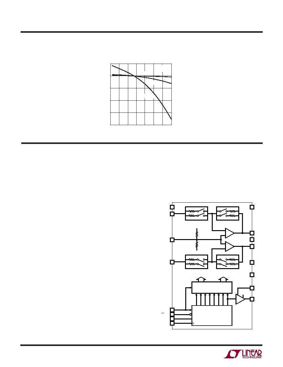
TYPICAL PERFOR A CE CHARACTERISTICS
UW
LTC6912-2 Gain Shift vs
Temperature (Heavy Load)
TEMPERATURE (°C)
–50
25
75
–25
0
50
100
125
GAIN
CHANGE
(dB)
0.25
0
–0.25
–0.50
–0.75
–1.00
6912 G26
VS = 5V
RL = 500
GAIN = 1
GAIN = 8
GAIN = 64
相关PDF资料 |
PDF描述 |
|---|---|
| LT1999IMS8-10#TRPBF | IC OP AMP CURRENT SENSE 8MSOP |
| LT1999IS8-50#TRPBF | IC AMP CURR SENSE HV 8-SOIC |
| LT1999IS8-20#TRPBF | IC AMP CURR SENSE HV 8-SOIC |
| LT1999IS8-10#TRPBF | IC AMP CURR SENSE HV 8-SOIC |
| LT1999IMS8-50#TRPBF | IC AMP CURR SENSE HV 8-MSOP |
相关代理商/技术参数 |
参数描述 |
|---|---|
| LTC6912CGN-2 | 制造商:Linear Technology 功能描述:SP Amp Variable Gain Amp Dual R-R I/O 制造商:Linear Technology 功能描述:SP Amp Variable Gain Amp Dual R-R I/O ±5.25V/10.5V 16-Pin SSOP N |
| LTC6912CGN-2#PBF | 功能描述:IC PGA DIGITAL R-R DUAL 16SSOP RoHS:是 类别:集成电路 (IC) >> Linear - Amplifiers - Instrumentation 系列:- 标准包装:50 系列:LinCMOS™ 放大器类型:通用 电路数:4 输出类型:- 转换速率:0.05 V/µs 增益带宽积:110kHz -3db带宽:- 电流 - 输入偏压:0.7pA 电压 - 输入偏移:210µV 电流 - 电源:57µA 电流 - 输出 / 通道:30mA 电压 - 电源,单路/双路(±):3 V ~ 16 V,±1.5 V ~ 8 V 工作温度:-40°C ~ 85°C 安装类型:表面贴装 封装/外壳:14-SOIC(0.154",3.90mm 宽) 供应商设备封装:14-SOIC 包装:管件 产品目录页面:865 (CN2011-ZH PDF) 其它名称:296-1834296-1834-5 |
| LTC6912CGN-2#TRPBF | 功能描述:IC PGA DIGITAL R-R DUAL 16SSOP RoHS:是 类别:集成电路 (IC) >> Linear - Amplifiers - Instrumentation 系列:- 标准包装:50 系列:LinCMOS™ 放大器类型:通用 电路数:4 输出类型:- 转换速率:0.05 V/µs 增益带宽积:110kHz -3db带宽:- 电流 - 输入偏压:0.7pA 电压 - 输入偏移:210µV 电流 - 电源:57µA 电流 - 输出 / 通道:30mA 电压 - 电源,单路/双路(±):3 V ~ 16 V,±1.5 V ~ 8 V 工作温度:-40°C ~ 85°C 安装类型:表面贴装 封装/外壳:14-SOIC(0.154",3.90mm 宽) 供应商设备封装:14-SOIC 包装:管件 产品目录页面:865 (CN2011-ZH PDF) 其它名称:296-1834296-1834-5 |
| LTC6912HGN-1 | 制造商:LINER 制造商全称:Linear Technology 功能描述:Dual Programmable Gain Amplifiers with Serial Digital Interface |
| LTC6912HGN-1#PBF | 功能描述:IC PGA DIGITAL R-R DUAL 16SSOP RoHS:是 类别:集成电路 (IC) >> Linear - Amplifiers - Instrumentation 系列:- 标准包装:2,500 系列:- 放大器类型:通用 电路数:1 输出类型:满摆幅 转换速率:0.11 V/µs 增益带宽积:350kHz -3db带宽:- 电流 - 输入偏压:4nA 电压 - 输入偏移:20µV 电流 - 电源:260µA 电流 - 输出 / 通道:20mA 电压 - 电源,单路/双路(±):2.7 V ~ 36 V,±1.35 V ~ 18 V 工作温度:-40°C ~ 85°C 安装类型:表面贴装 封装/外壳:8-SOIC(0.154",3.90mm 宽) 供应商设备封装:8-SO 包装:带卷 (TR) |
发布紧急采购,3分钟左右您将得到回复。