参数资料
| 型号: | LTC6915IGN |
| 厂商: | Linear Technology |
| 文件页数: | 7/18页 |
| 文件大小: | 0K |
| 描述: | IC PGA DIGITAL PREC 0DRFT 16SSOP |
| 标准包装: | 100 |
| 放大器类型: | 仪表 |
| 电路数: | 1 |
| 输出类型: | 满摆幅 |
| 转换速率: | 0.2 V/µs |
| 增益带宽积: | 200kHz |
| 电流 - 输入偏压: | 4nA |
| 电压 - 输入偏移: | 5µV |
| 电流 - 电源: | 1.73mA |
| 电压 - 电源,单路/双路(±): | 2.7 V ~ 11 V,±1.35 V ~ 5.5 V |
| 工作温度: | -40°C ~ 85°C |
| 安装类型: | 表面贴装 |
| 封装/外壳: | 16-SSOP(0.154",3.90mm 宽) |
| 供应商设备封装: | 16-SSOP |
| 包装: | 管件 |
LTC6915
15
6915fb
operaTion
Settling Time
The sampling rate is 3kHz and the input sampling period
duringwhichCSischargedtotheinputdifferentialvoltage,
VIN, is approximately 150s. First assume that on each
input sampling period, CS is charged fully to VIN. Since
CS = CH (= 1000pF), a change in the input will settle to
N bits of accuracy at the op amp noninverting input after
N clock cycles or 333s(N). The settling time at the OUT
pin is also affected by the internal op amp. Since the gain
bandwidth of the internal op amp is typically 200kHz, the
settling time is dominated by the switched-capacitor front
end for gains below 100 (see the Low Gain Settling Time
vs Settling Accuracy and the Settling Time vs Gain graphs
in the Typical Performance Characteristics section). In ad-
dition, the worst case settling time after a device-enable
(activelowonPin1ofaGNpackage)isequaltothesettling
due to the gain plus the input settling time (333s N).
For example, if an LTC6915 is enabled with a logic high on
Pin 1 then, the maximum settling time to 10 bits of ac-
curacy (0.1%) and a gain equal to 100 is 8.33ms ([333s
1024] + 5ms).
Input Current
Whenever the differential input VIN changes, CH must be
charged up to the new input voltage via CS. This results
in an input charging current during each input sampling
period. Eventually, CH and CS will reach VIN and ideally,
the input current would go to zero for DC inputs.
In reality, there are additional parasitic capacitors which
disturb the charge on CS every cycle even if VIN is a DC
voltage. For example, the parasitic bottom plate capacitor
on CS must be charged from the voltage on the REF pin to
the voltage on the IN– pin every cycle. The resulting input
charging current decays exponentially during each input
sampling period with a time constant equal to RSCS. If the
voltage disturbance due to these currents settles before
the end of the sampling period, there will be no errors due
to source resistance or the source resistance mismatch
between IN+ and IN–. With RS less than 10k, no DC errors
occur due to input current mismatch.
In the Typical Performance Characteristics section of this
data sheet, there are curves showing the additional error
from non-zero source resistance in the inputs. If there
are no large capacitors across the inputs, the amplifier is
less sensitive to source resistance and source resistance
mismatch. When large capacitors are placed across the
inputs, the input charging currents are placed across
the inputs. The input charging currents described above
result in larger DC errors, especially with source resistor
mismatches.
Power Supply Bypassing
In a dual supply operation, connect a 0.1F bypass ca-
pacitor from each power supply pin (V+ and V–) to an
analog round plance surrounding an LTC6915. The bypass
capacitor trace to the supply pins must be less than
0.2inches(anX7RorX5Rcapacitortypeisrecommended).
Insinglesupplyoperation,connecttheV–pintotheanalog
ground plane and bypass the V+ pin.
Shutdown Modes
The IC has two shutdown modes, hardware shutdown and
software shutdown. When SHDN is tied to V+, the IC is in
hardware shutdown mode. During this shutdown mode,
the gain setting digital interface (serial or parallel) and the
main op amp are both disabled, thus the PGA dissipates
very small supply current (see the Electrical Characteristic
table). When SHDN is floating, an internal current source
will pull it down to V–. The digital interface is turned on to
read the gain setting codes. The IC is in normal amplifica-
tion mode as long as the gain control code is other than
0000. If the gain control code is 0000, the IC operates in
software shutdown mode, i.e., the main op amp is turned
offsothatthePGAdissipateslesspower.TheDFNpackage
does not have hardware shutdown.
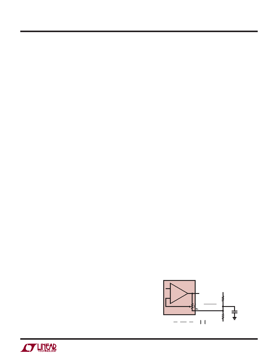
Setting the Voltage at the REF Pin
The current coming out of the REF pin may affect the
reference voltage at the REF pin (VREF). If VREF is set by
a resistive divider then the VREF voltage is a function of
the VOUT voltage (see Figure 5). In order to minimize the
VREF variations, the total resistance of R1 plus R2 should
be much less than 32k (5k or less) or use a voltage refer-
ence to set VREF.
Figure 5
–
+
REF
IREF =
VOUT – VREF
32k
VOUT
V+
V–
R1
R2
LTC6915
R = 32k
6915 F05
V
R
V
k
V
R
RR
k
REF
OUT
=+
+
+
12
32
–
(
)
VREF
0.1F
OUT
相关PDF资料 |
PDF描述 |
|---|---|
| TMM-129-01-T-D-SM | CONN HEADER 58POS DUAL 2MM SMD |
| SSQ-104-03-S-D-RA | CONN RCPT .100" 8POS DL R/A GOLD |
| LTC6915IDE#PBF | IC PGA DIGITAL PREC 0DRFT 12DFN |
| SSQ-105-03-S-D-RA | CONN RCPT .100" 10PS DL R/A GOLD |
| TMM-123-01-G-S-SM | CONN HEADER 23POS SNGL 2MM SMD |
相关代理商/技术参数 |
参数描述 |
|---|---|
| LTC6915IGN#PBF | 功能描述:IC PGA DIGITAL PREC 0DRFT 16SSOP RoHS:否 类别:集成电路 (IC) >> Linear - Amplifiers - Instrumentation 系列:- 标准包装:1 系列:- 放大器类型:通用 电路数:4 输出类型:满摆幅 转换速率:0.028 V/µs 增益带宽积:105kHz -3db带宽:- 电流 - 输入偏压:3nA 电压 - 输入偏移:100µV 电流 - 电源:3.3µA 电流 - 输出 / 通道:12mA 电压 - 电源,单路/双路(±):2.7 V ~ 12 V,±1.35 V ~ 6 V 工作温度:-40°C ~ 85°C 安装类型:表面贴装 封装/外壳:14-TSSOP(0.173",4.40mm 宽) 供应商设备封装:14-TSSOP 包装:剪切带 (CT) 其它名称:OP481GRUZ-REELCT |
| LTC6915IGN#PBF | 制造商:Linear Technology 功能描述:INSTR-AMPLIFIER 200KHZ 125DB 制造商:Linear Technology 功能描述:INSTR-AMPLIFIER 200KHZ 125DB SSOP-16 制造商:Linear Technology 功能描述:INSTR-AMPLIFIER, 200KHZ, 125DB, SSOP-16 |
| LTC6915IGN#TR | 功能描述:IC PGA DIGITAL PREC 0DRFT 16SSOP RoHS:否 类别:集成电路 (IC) >> Linear - Amplifiers - Instrumentation 系列:- 标准包装:100 系列:- 放大器类型:通用 电路数:1 输出类型:- 转换速率:0.2 V/µs 增益带宽积:- -3db带宽:- 电流 - 输入偏压:100pA 电压 - 输入偏移:30µV 电流 - 电源:380µA 电流 - 输出 / 通道:- 电压 - 电源,单路/双路(±):±2 V ~ 18 V 工作温度:0°C ~ 70°C 安装类型:表面贴装 封装/外壳:8-SOIC(0.154",3.90mm 宽) 供应商设备封装:8-SO 包装:管件 |
| LTC6915IGN#TRPBF | 功能描述:IC PGA DIGITAL PREC 0DRFT 16SSOP RoHS:是 类别:集成电路 (IC) >> Linear - Amplifiers - Instrumentation 系列:- 标准包装:100 系列:- 放大器类型:通用 电路数:1 输出类型:- 转换速率:0.2 V/µs 增益带宽积:- -3db带宽:- 电流 - 输入偏压:100pA 电压 - 输入偏移:30µV 电流 - 电源:380µA 电流 - 输出 / 通道:- 电压 - 电源,单路/双路(±):±2 V ~ 18 V 工作温度:0°C ~ 70°C 安装类型:表面贴装 封装/外壳:8-SOIC(0.154",3.90mm 宽) 供应商设备封装:8-SO 包装:管件 |
| LTC691C | 制造商:LINER 制造商全称:Linear Technology 功能描述:Microprocessor Supervisory Circuits |
发布紧急采购,3分钟左右您将得到回复。