参数资料
| 型号: | LTC6994IS6-1#TRPBF |
| 厂商: | Linear Technology |
| 文件页数: | 26/26页 |
| 文件大小: | 0K |
| 描述: | IC DELAY LINE TSOT-23-6 |
| 产品培训模块: | TimerBlox Family Timing Devices |
| 特色产品: | TimerBlox? |
| 标准包装: | 2,500 |
| 系列: | TimerBlox® |
| 功能: | 可编程 |
| 可用的总延迟: | 1µs ~ 33.6s |
| 独立延迟数: | 1 |
| 电源电压: | 2.25 V ~ 5.5 V |
| 工作温度: | -40°C ~ 85°C |
| 安装类型: | 表面贴装 |
| 封装/外壳: | SOT-23-6 细型,TSOT-23-6 |
| 供应商设备封装: | TSOT-23-6 |
| 包装: | 带卷 (TR) |
| 配用: | DC1562A-E-ND - BOARD EVAL LTC6992-3 |
LTC6994-1/LTC6994-2
9
699412fb
pin FuncTions (DCB/S6)
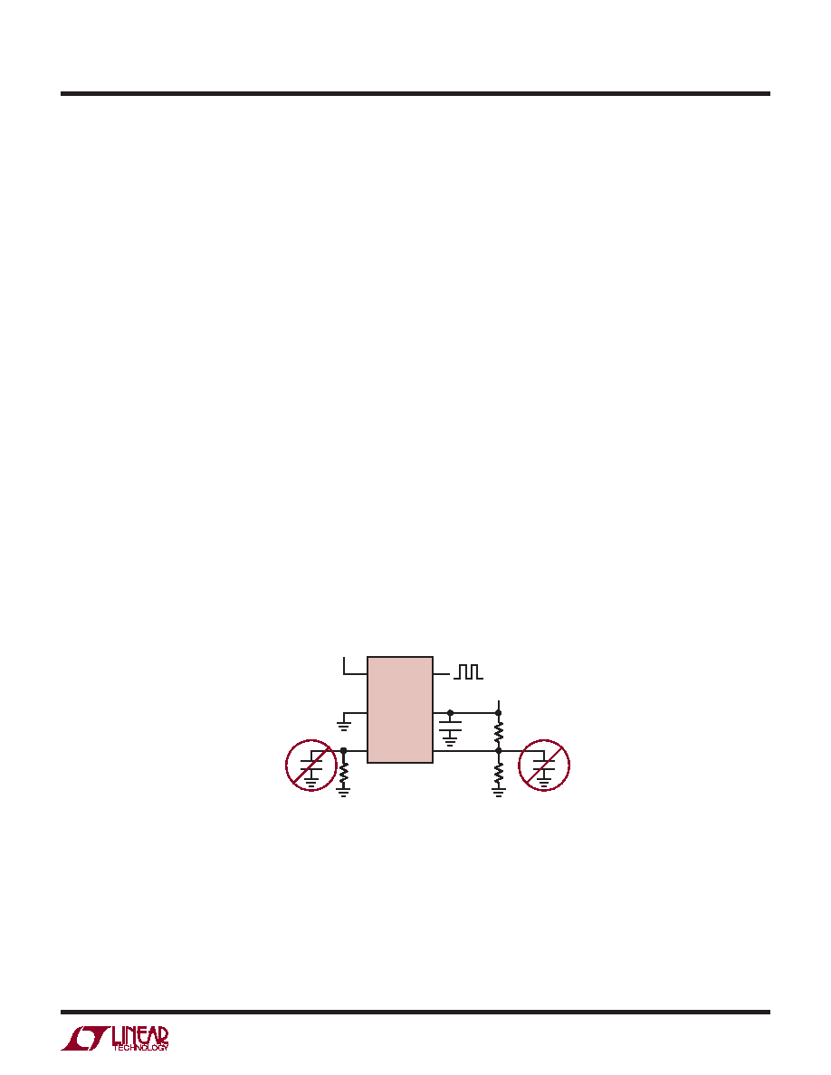
V+ (Pin 1/Pin 5): Supply Voltage (2.25V to 5.5V). This sup-
ply should be kept free from noise and ripple. It should be
bypassed directly to the GND pin with a 0.1F capacitor.
DIV (Pin 2/Pin 4): Programmable Divider and Polarity
Input. The DIV pin voltage (VDIV) is internally converted
into a 4-bit result (DIVCODE). VDIV may be generated by
a resistor divider between V+ and GND. Use 1% resistors
to ensure an accurate result. The DIV pin and resistors
should be shielded from the OUT pin or any other traces
that have fast edges. Limit the capacitance on the DIV pin
to less than 100pF so that VDIV settles quickly. The MSB
of DIVCODE (POL) selects the delay functionality. For the
LTC6994-1, POL = 0 will delay the rising transition and
POL = 1 will delay the falling transition. For the LTC6994-
2, both transitions are delayed so POL = 1 can be used
to invert the output.
SET (Pin 3/Pin 3): Delay Setting Input. The voltage on the
SET pin (VSET) is regulated to 1V above GND. The amount
of current sourced from the SET pin (ISET) programs the
master oscillator frequency. The ISET current range is
1.25A to 20A. The delayed output transition will be not
occur if ISET drops below approximately 500nA. Once ISET
increases above 500nA the delayed edge will transition.
A resistor connected between SET and GND is the most
accurate way to set the delay. For best performance, use
a precision metal or thin film resistor of 0.5% or better
tolerance and 50ppm/°C or better temperature coefficient.
For lower accuracy applications an inexpensive 1% thick
film resistor may be used.
Limit the capacitance on the SET pin to less than 10pF
to minimize jitter and ensure stability. Capacitance less
than 100pF maintains the stability of the feedback circuit
regulating the VSET voltage.
IN(Pin4/Pin1):LogicInput.Dependingontheversionand
POL bit setting, rising or falling edges on IN will propagate
to OUT after a programmable delay. The LTC6994-1 will
delay only the rising or falling edge. The LTC6994-2 will
delay both edges.
GND (Pin 5/Pin 2): Ground. Tie to a low inductance ground
plane for best performance.
OUT (Pin 6/Pin 6): Output. The OUT pin swings from
GND to V+ with an output resistance of approximately
30Ω. When driving an LED or other low impedance load
a series output resistor should be used to limit source/
sink current to 20mA.
699412 PF
LTC6994
IN
GND
SET
OUT
V+
DIV
C1
0.1F
RSET
R2
R1
V+
相关PDF资料 |
PDF描述 |
|---|---|
| VI-BND-IU-F1 | CONVERTER MOD DC/DC 85V 200W |
| LTC6994IS6-1#TRMPBF | IC DELAY LINE TSOT-23-6 |
| VI-B6N-IU-F4 | CONVERTER MOD DC/DC 18.5V 200W |
| VI-BWN-MV | CONVERTER MOD DC/DC 18.5V 150W |
| VI-B6N-IU-F3 | CONVERTER MOD DC/DC 18.5V 200W |
相关代理商/技术参数 |
参数描述 |
|---|---|
| LTC6994IS6-2#PBF | 制造商:Linear Technology 功能描述:Programmable Delay Block 6-Pin TSOT-23 制造商:Linear Technology 功能描述:SC-Timing, Cut Tape Delay with Rising and Falling Edge Trigger |
| LTC6994IS6-2#TRM | 制造商:Linear Technology 功能描述:Programmable Delay Block 6-Pin TSOT-23 T/R |
| LTC6994IS6-2#TRMPBF | 功能描述:IC DELAY LINE TSOT-23-6 RoHS:是 类别:集成电路 (IC) >> 时钟/计时 - 延迟线 系列:TimerBlox® 标准包装:2,500 系列:- 标片/步级数:- 功能:多个,不可编程 延迟到第一抽头:10ns 接头增量:- 可用的总延迟:10ns 独立延迟数:4 电源电压:4.75 V ~ 5.25 V 工作温度:0°C ~ 70°C 安装类型:表面贴装 封装/外壳:14-SOIC(0.154",3.90mm 宽) 供应商设备封装:14-SOIC 包装:带卷 (TR) |
| LTC6994IS6-2#TRPBF | 功能描述:IC DELAY LINE TSOT-23-6 RoHS:是 类别:集成电路 (IC) >> 时钟/计时 - 延迟线 系列:TimerBlox® 标准包装:2,500 系列:- 标片/步级数:- 功能:多个,不可编程 延迟到第一抽头:10ns 接头增量:- 可用的总延迟:10ns 独立延迟数:4 电源电压:4.75 V ~ 5.25 V 工作温度:0°C ~ 70°C 安装类型:表面贴装 封装/外壳:14-SOIC(0.154",3.90mm 宽) 供应商设备封装:14-SOIC 包装:带卷 (TR) |
| LTC6994IS6-2TRMPBF | 制造商:LINER 制造商全称:Linear Technology 功能描述:TimerBlox: Delay Block/ Debouncer |
发布紧急采购,3分钟左右您将得到回复。