参数资料
| 型号: | LV5781-TLM-E |
| 厂商: | ON Semiconductor |
| 文件页数: | 5/7页 |
| 文件大小: | 0K |
| 描述: | IC REG BUCK 3.3V 3A 14HSSOP |
| 标准包装: | 2,000 |
| 类型: | 降压(降压) |
| 输出类型: | 固定 |
| 输出数: | 1 |
| 输出电压: | 3.3V |
| 输入电压: | 4.5 V ~ 6 V |
| 频率 - 开关: | 180kHz |
| 电流 - 输出: | 3A |
| 同步整流器: | 无 |
| 工作温度: | -30°C ~ 80°C |
| 安装类型: | 表面贴装 |
| 封装/外壳: | 20-LSSOP(0.173",4.40mm 宽)16 引线 |
| 包装: | 带卷 (TR) |
| 供应商设备封装: | 14-HSSOP |
�� �
�
�LV5781�
�Pin� Functions�
�Pin� No.�
�1�
�2�
�3�
�4�
�5,� 8,� 10�
�6,� 9�
�7�
�11�
�12�
�13�
�14�
�Heat� sink� fin�
�Pin� name�
�FB_GND�
�ENABLE�
�SS�
�FB1�
�VIN�
�SW�
�PGND�
�CBOOT�
�OERRAMP�
�FB2�
�FB0�
�GND�
�Description�
�GND� of� output� voltage� setting� pins� FB0� and� FB2.� It� is� connected� to� GND� for� use� when� pin� FB2� is� used.�
�Output� ON/OFF� with� an� active-high� polarity.� When� set� to� L,� the� current� consumption� is� reduced� to� 10� μ� A� or�
�less.�
�Soft� start� time� constant� setting.� The� charge� current� is� set� to� approx.� 6.5� μ� A� and� when� a� capacitor� of� 0.1� μ� F� is�
�connected� between� this� pin� and� GND,� the� output� rises� in� approx.� 12ms.�
�Test� pin� for� verifying� the� internal� reference� voltage.� It� must� be� set� to� open� for� actual� use.�
�Power� input.� It� is� used� with� voltages� ranging� from� 4.5V� to� 6V.�
�Inductor� drive� output�
�Power� GND� pin.� This� is� the� output� GND.� It� is� connected� so� that� where� at� all� possible,� no� impedance� is�
�shared� with� other� GND� pins� (GND,� FB_GND).�
�For� generating� the� gate� voltage� of� the� internal� high-side� n-channel� MOS� transistor.� A� capacitor� with� a�
�capacitance� of� at� least� 0.1� μ� F� (max.� 2.2� μ� F)� is� connected� between� this� pin� and� the� SW� pin� for� use.�
�Transconductance-type� Error_Amp� output.� An� integration� constant� is� provided� between� this� pin� and� GND� to�
�implement� phase� compensation.�
�Used� to� feed� back� the� output� voltage� to� this� pin� when� the� output� voltage� is� to� be� set� to� 3.3V.� In� such� a� case,�
�FB_GND� is� connected� to� GND.� Refer� to� application� circuit� 1.�
�When� the� output� voltage� is� to� be� set� to� a� desired� value,� connect� resistors� between� FB0� and� GND� and�
�between� FB0� and� VOUT� to� feed� back� the� output� voltage� to� this� pin.� In� such� a� case,� leave� FB_GND� and�
�FB2� open.� Refer� to� application� circuit� 2.�
�Analog� GND� (connected� to� GND).�
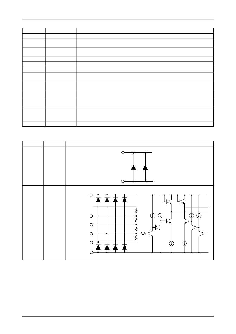
�Input� Equivalent� Circuits�
�Pin� No.�
�5,� 8,� 10�
�1�
�4�
�13�
�14�
�Pin� Name�
�GND�
�VIN�
�FB_GND�
�FB1�
�FB2�
�FB0�
�VIN�
�FB2�
�FB1�
�FB0�
�FB_GND�
�GND�
�VIN�
�GND�
�Equivalent� Circuit�
�116k� Ω�
�50k� Ω�
�118k� Ω�
�54.5k� Ω�
�Continued� on� next� page�
�No.A0663-5/7�
�相关PDF资料 |
PDF描述 |
|---|---|
| LV5857MX-TLM-H | IC REG BUCK SYNC ADJ 3A MFP8 |
| LV5876MX-TLM-H | IC REG BUCK SYNC ADJ 2A MFP8 |
| LV8773-E | IC MOTOR DVR PWM CC 2CH 28-DIP |
| M14BCK | CONN BUTT UNINSUL 16-14 AWG |
| M20-6103205 | CONN HDR FMALE .100" 64POS AU |
相关代理商/技术参数 |
参数描述 |
|---|---|
| LV5803M | 制造商:SANYO 制造商全称:Sanyo Semicon Device 功能描述:Bi-CMOS IC Step-down Switching Regulator |
| LV5803M-TE-L-E | 功能描述:直流/直流开关调节器 SWITCHING REGULATOR RoHS:否 制造商:International Rectifier 最大输入电压:21 V 开关频率:1.5 MHz 输出电压:0.5 V to 0.86 V 输出电流:4 A 输出端数量: 最大工作温度: 安装风格:SMD/SMT 封装 / 箱体:PQFN 4 x 5 |
| LV58061MX | 制造商:SANYO 制造商全称:Sanyo Semicon Device 功能描述:Step-down Switching Regulator |
| LV58061MX-TLM-H | 功能描述:直流/直流开关调节器 SWITCHING REGULATOR RoHS:否 制造商:International Rectifier 最大输入电压:21 V 开关频率:1.5 MHz 输出电压:0.5 V to 0.86 V 输出电流:4 A 输出端数量: 最大工作温度: 安装风格:SMD/SMT 封装 / 箱体:PQFN 4 x 5 |
| LV58063MC | 制造商:SANYO 制造商全称:Sanyo Semicon Device 功能描述:Step-down Switching Regulator |
发布紧急采购,3分钟左右您将得到回复。