- 您现在的位置:买卖IC网 > PDF目录369877 > LX1672-06CLQ RADIATION HARDENED HIGH EFFICIENCY, 5 AMP SWITCHING REGULATORS PDF资料下载
参数资料
| 型号: | LX1672-06CLQ |
| 元件分类: | 基准电压源/电流源 |
| 英文描述: | RADIATION HARDENED HIGH EFFICIENCY, 5 AMP SWITCHING REGULATORS |
| 中文描述: | 抗辐射高效,5安培开关稳压器 |
| 文件页数: | 12/21页 |
| 文件大小: | 554K |
| 代理商: | LX1672-06CLQ |
Microsemi
Integrated Products, Power Management
11861 Western Avenue, Garden Grove, CA. 92841, 714-898-8121, Fax: 714-893-2570
Page 12
Copyright
2000
Rev. 0.5i, 2002-07-17
W
M
.
C
LX1671
Multiple Output LoadSHARE PWM
P
RELIMINARY
I N T E G R A T E D P R O D U C T S
THEORY OF OPERATION
(CONTINUED)
B
I
-P
HASE
, L
OAD
SHARE (ESR M
ETHOD
)
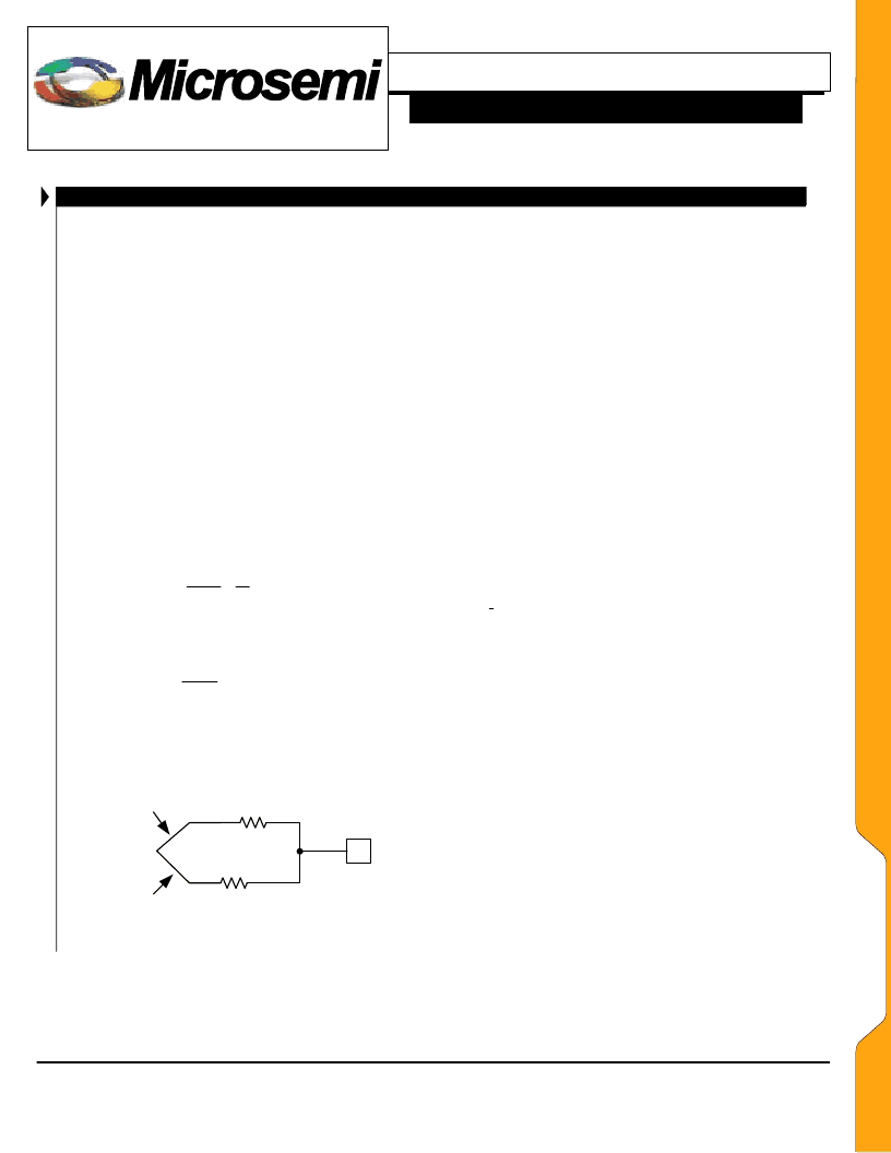
The first method is to change the ratio of the inductors
equivalent series resistance, (ESR). As can be seen in the
previous example, if the offset error is zero and the ESR of the
two inductors are identical, then the two inductor currents will be
identical. To change the ratio of current between the two
inductors, the value of the inductor’s ESR can be changed to
allow more current to flow through one inductor than the other.
The inductor with the lower ESR value will have the larger
current. The inductor currents are directly proportional to the
ratio of the inductor’s ESR value.
The following circuit description shows how to select the
inductor ESR for each phase where a different amount of power
is taken from two different input power supplies. A typical setup
will have a +5V power supply connected to the phase 1 half
bridge driver and a +3.3V power supply connected to the phase 2
half bridge driver. The combined power output for this core
voltage is 18W (+1.5V @ 12A). For this example the +5V power
supply will supply 7W and the +3.3V power supply will supply
the other 11W. 7W @ 1.5V is a 4.67A current through the phase
1 inductor. 11W @ 1.5V is a 7.33A current through the phase 2
inductor. The ratio of inductor ESR is inversely proportional to
2
2
ESR
the power level split.
1
1
ESR
=
The higher current inductor will have the lower ESR value. If the
ESR of the phase 1 inductor is selected as 10m
, then the ESR
value of the phase 2 inductor is calculated as:
m
4
m
10
A
33
.
A
67
.
=
×
Depending on the required accuracy of this power sharing;
inductors can be chosen from standard vendor tables with an ESR
ratio close to the required values. Inductors can also be designed
for a given application so that there is the least amount of
compromise in the inductor’s performance.
1.5V @ 12A
7.33A
18W
6.4m
4.67A
10m
1.5V +
46.7mV
L1
L2
+5V @ 7W
+3.3V @ 11W
Figure 7
–LoadSHARE Using Inductor ESR
B
I
-P
HASE
, L
OAD
SHARE (F
EEDBACK
D
IVIDER
M
ETHOD
)
Sometimes it is desirable to use the same inductor in both
phases while having a much larger current in one phase versus the
other. A simple resistor divider can be used on the input side of
the Low Pass Filter that is taken off of the switching side of the
inductors. If the Phase 2 current is to be larger than the current in
Phase 1; the resistor divider is placed in the feedback path before
the Low Pass Filter that is connected to the Phase 2 inductor. If the
Phase 2 current needs to be less than the current in Phase 1; the
resistor divider is then placed in the feedback path before the Low
Pass Filter that is connected to the Phase 1 inductor.
As in Figure 7, the millivolts of DC offset created by the
resistor divider network in the feedback path, appears as a voltage
generator between the ESR of the two inductors.
A divider in the feedback path from Phase 2 will cause the
voltage generator to be positive at Phase 2. With a divider in the
feedback path of Phase 1 the voltage generator becomes positive at
Phase 1. The Phase with the positive side of the voltage generator
will have the larger current. Systems that operate continuously
above a 30% power level can use this method, a down side is that
the current difference between the two inductors still flows during
a no load condition.
This produces a low efficiency condition during a no load or
light load state, this method should not be used if a wide range of
output power is required.
The following description and Figure 8 show how to determine
the value of the resistor divider network required to generate the
offset voltage necessary to produce the different current ratio in the
two output inductors. The power sharing ratio is the same as that
of Figure 7. The Offset Voltage Generator is symbolic for the DC
voltage offset between Phase 1 & 2. This voltage is generated by
small changes in the duty cycle of Phase 2. The output of the LPF
is a DC voltage proportional to the duty cycle on its input. A small
amount of attenuation by a resistor divider before the LPF of Phase
2 will cause the duty cycle of Phase 2 to increase to produce the
added offset at V2. The high DC gain of the error amplifier will
force LPF2 to always be equal to LPF1. The following
calculations determine the value of the resistor divider necessary to
satisfy this example.
A
P
P
L
I
C
A
T
I
O
N
S
相关PDF资料 |
PDF描述 |
|---|---|
| LX1673-03CLQ | PWM Controllers |
| LX1673-03CPW | PWM Controllers |
| LX1673-06CLQ | PWM Controllers |
| LX1673-06CPW | PWM Controllers |
| LX1673-09CLQ | PWM Controllers |
相关代理商/技术参数 |
参数描述 |
|---|---|
| LX1672-06CLQ-TR | 制造商:Microsemi Corporation 功能描述:MOSFET DRVR 0.8V 1A 3-OUT HI/LO SIDE HALF BRDG NON-INV 38MLP - Tape and Reel |
| LX1673 | 制造商:MICROSEMI 制造商全称:Microsemi Corporation 功能描述:High Frequency PWM Regulator |
| LX1673-03CLQ | 功能描述:IC REG DL BCK/LINEAR SYNC 20MLPQ RoHS:是 类别:集成电路 (IC) >> PMIC - 稳压器 - 线性 + 切换式 系列:- 标准包装:2,500 系列:- 拓扑:降压(降压)同步(2),线性(LDO)(1) 功能:任何功能 输出数:3 频率 - 开关:300kHz 电压/电流 - 输出 1:控制器 电压/电流 - 输出 2:控制器 电压/电流 - 输出 3:控制器 带 LED 驱动器:无 带监控器:无 带序列发生器:是 电源电压:4.5 V ~ 24 V 工作温度:-40°C ~ 85°C 安装类型:* 封装/外壳:28-TSSOP(0.173",4.40mm 宽) 供应商设备封装:* 包装:带卷 (TR) 其它名称:ISL6402IVZ-TTR |
| LX1673-03CLQ-TR | 制造商:Microsemi Corporation 功能描述:VOLT MODE PWM CNTRLR 0.8V TO 5.5V 1A 20MLPQ - Tape and Reel |
| LX1673-03CPW | 功能描述:IC REG DL BCK/LINEAR 20TSSOP RoHS:是 类别:集成电路 (IC) >> PMIC - 稳压器 - 线性 + 切换式 系列:- 标准包装:2,500 系列:- 拓扑:降压(降压)同步(2),线性(LDO)(1) 功能:任何功能 输出数:3 频率 - 开关:300kHz 电压/电流 - 输出 1:控制器 电压/电流 - 输出 2:控制器 电压/电流 - 输出 3:控制器 带 LED 驱动器:无 带监控器:无 带序列发生器:是 电源电压:4.5 V ~ 24 V 工作温度:-40°C ~ 85°C 安装类型:* 封装/外壳:28-TSSOP(0.173",4.40mm 宽) 供应商设备封装:* 包装:带卷 (TR) 其它名称:ISL6402IVZ-TTR |
发布紧急采购,3分钟左右您将得到回复。