- 您现在的位置:买卖IC网 > PDF目录39438 > LX7203-22ISMTR (MICROSEMI CORP-ANALOG MIXED SIGNAL GROUP) 2 FUNCTIONS, 5.25 V, DATA LINE FILTER PDF资料下载
参数资料
| 型号: | LX7203-22ISMTR |
| 厂商: | MICROSEMI CORP-ANALOG MIXED SIGNAL GROUP |
| 元件分类: | 数据传输滤波器 |
| 英文描述: | 2 FUNCTIONS, 5.25 V, DATA LINE FILTER |
| 文件页数: | 2/7页 |
| 文件大小: | 250K |
| 代理商: | LX7203-22ISMTR |
LX7203-xx
PRODUCTION DATA SHEET
Microsemi
Integrated Products Division
11861 Western Avenue, Garden Grove, CA. 92841, 714-898-8121, Fax: 714-893-2570
Page 2
WWW
.Microse
m
i
.CO
M
EMI Filter & ESD Protection for Up Stream USB
Ports
Copyright
2002
Rev. 1.1d, 2005-05-18
TM
ABSOLUTE MAXI MUM RATI NGS
Steady State Power ................................................................100mW
ESD Air Discharge per IEC61000-4-2.......................................16kV
ESD Contact Discharge per IEC61000-4-2 ...............................10kV
Peak Package Solder Reflow Temperature
(40 second maximum exposure) ................................. 260°C (+0, -5)
Operating Temperature ............................................-40°C to +125°C
Storage Temperature Range.....................................-65°C to +150°C
Note: Exceeding these ratings could cause damage to the device. All voltages are
with
respect to
Ground. Currents are positive into, negative out of specified
terminal
.
TH ERM A L DATA
SM Plastic 6-Pin SC70
THERMAL RESISTANCE
-JUNCTION TO CASE,
θJC
119
°C/W
THERMAL RESISTANCE
-JUNCTION TO AMBIENT,
θJA 122 °C/W
Junction Temperature Calculation: TJ = TA + (PD x θJA).
The θJA numbers are guidelines for the thermal performance of the device/pc-board
system. All of the above assume no ambient airflow.
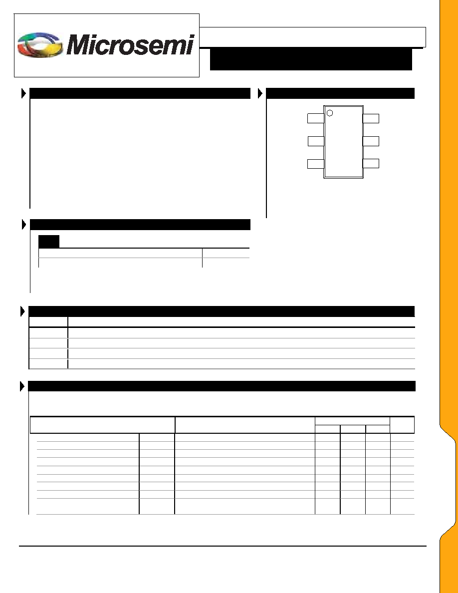
PACKAGE PI N OUT
V
BUS
D
IN
D
IN
D
OUT
D
OUT
GND
1
2
3
4
5
6
from
connector
from
connector
to IC
SM PACKAGE
(Top View)
RoHS / Pb-free 100% Matte Tin Lead Finish
FUNCTIONAL PIN DESCRIPTION
Name
Description
VBUS
Bus Voltage
DIN
Data In
GND
Ground
DOUT
Data Out
ELECTRI CAL CHA RACTERI S TI CS
Unless otherwise specified, the following specifications apply over the operating ambient temperature -40°C
≤ TA ≤ +125°C except where
otherwise noted.
LX7203
Parameter
Symbol
Test Conditions
Min
Typ
Max
Units
Stand-Off Voltage
VRWM
5.25
V
Breakdown Voltage
VBR
IR = 1mA
6
V
Leakage Current
IR
VRWM = 5.25V, T = 25°C
1
A
Series Resistance (-15)
RS
Each Line
13.5
15
16.5
Series Resistance (-22)
RS
Each Line
19.8
22
24.2
Temperature Coefficient of RS
TCOEFF
Each Line
200
ppm
Pull Up Resistance
RPU
Each Line
1.35
1.5
1.65
K
Capacitor
CEDGE
Each Line
47
pF
Total Capacitance
CTOT
Between I/O Pins and Ground, Each Device
VR = 0V, f = 1MHz
54
60
66
pF
EE
LL
EE
CC
TT
RR
IICC
AA
LL
SS
相关PDF资料 |
PDF描述 |
|---|---|
| LX7203-15ISMT | 1 FUNCTIONS, DATA LINE FILTER |
| LX7203-22ISMT | 1 FUNCTIONS, DATA LINE FILTER |
| LX7205ISP | 2 FUNCTIONS, 5 V, DATA LINE FILTER |
| LX7207ISP | 1 FUNCTIONS, DATA LINE FILTER |
| LX7207ISP | 10 FUNCTIONS, DATA LINE FILTER |
相关代理商/技术参数 |
参数描述 |
|---|---|
| LX7203-XX | 制造商:MICROSEMI 制造商全称:Microsemi Corporation 功能描述:EMI Filter & ESD Protection for Up Stream USB Ports |
| LX-7204T-002AC | 制造商:MRV 制造商全称:MRV 功能描述:7304/7204 Sensor Manager |
| LX-7204T-012DC | 制造商:MRV 制造商全称:MRV 功能描述:7304/7204 Sensor Manager |
| LX7206 | 制造商:MICROSEMI 制造商全称:Microsemi Corporation 功能描述:Integrated EMI Filter & ESD Protection for Earpiece Speaker & Microphone Ports |
| LX723 | 制造商:POLYFET 制造商全称:Polyfet RF Devices 功能描述:SILICON GATE ENHANCEMENT MODE RF POWER LDMOS TRANSISTOR |
发布紧急采购,3分钟左右您将得到回复。