- 您现在的位置:买卖IC网 > PDF目录369885 > LXT363LE PCM TRANSCEIVER|SINGLE|T-1(DS1)|CMOS|QFP|44PIN|PLASTIC PDF资料下载
参数资料
| 型号: | LXT363LE |
| 英文描述: | PCM TRANSCEIVER|SINGLE|T-1(DS1)|CMOS|QFP|44PIN|PLASTIC |
| 中文描述: | 的PCM收发器|单|的T 1(DS1的)|的CMOS | QFP封装| 44PIN |塑料 |
| 文件页数: | 37/52页 |
| 文件大小: | 1187K |
| 代理商: | LXT363LE |
第1页第2页第3页第4页第5页第6页第7页第8页第9页第10页第11页第12页第13页第14页第15页第16页第17页第18页第19页第20页第21页第22页第23页第24页第25页第26页第27页第28页第29页第30页第31页第32页第33页第34页第35页第36页当前第37页第38页第39页第40页第41页第42页第43页第44页第45页第46页第47页第48页第49页第50页第51页第52页
Integrated T1/E1 LH/SH Transceiver for DS1/DSX-1 or PRI Applications
—
LXT361
Datasheet
37
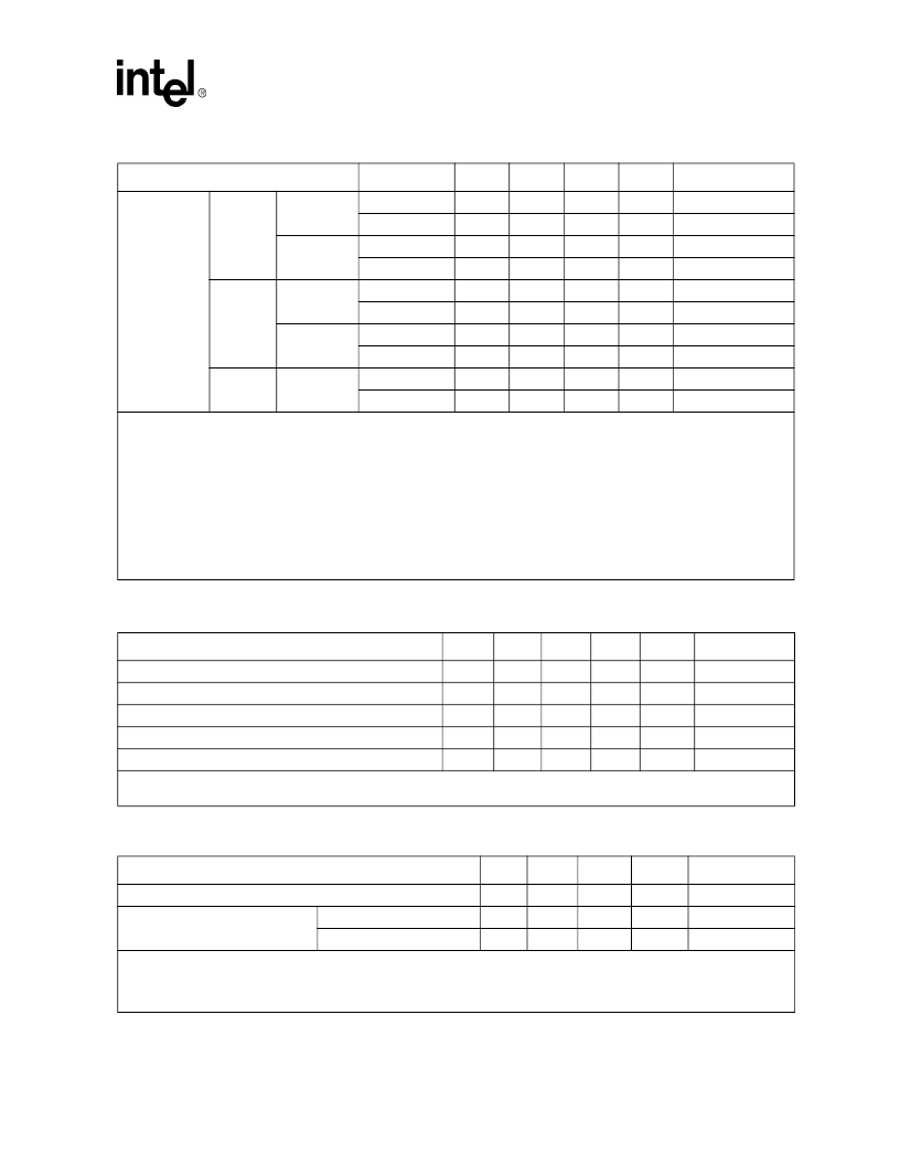
Total
power
dissipation
T1
3
low power
Short Haul
P
D
–
310
380
mW
100% mark density
P
D
–
225
295
mW
50% mark density
Long Haul
P
D
–
245
325
mW
100% mark density
P
D
–
195
265
mW
50% mark density
T1
4
standard
power
Short Haul
P
D
–
470
560
mW
100% mark density
P
D
–
320
380
mW
50% mark density
Long Haul
P
D
–
350
420
mW
100% mark density
P
D
–
260
310
mW
50% mark density
E1
5
Short Haul/
Long Haul
P
D
–
275
330
mW
100% mark density
P
D
–
215
270
mW
50% mark density
Table 25. Digital Characteristics
Parameter
Sym
Min
Typ
Max
Unit
Test Conditions
High level input voltage (pins 1-5, 9-12, 17, 23-28)
2
V
IH
2.0
–
–
V
Low level input voltage (pins 1-5, 9-12, 17, 23-28)
2
V
IL
–
–
0.8
V
High level output voltage
1
(pins 6-8, 10, 11,23, 28)
2
V
OH
2.4
–
–
V
I
OUT
= 400
μ
A
Low level output voltage
1
(pins 6-8, 10, 11,23, 28)
2
V
OL
–
–
0.4
V
I
OUT
= 1.6 mA
Input leakage current
I
LL
–
–
±50
μ
A
1. Output drivers will output CMOS logic levels into CMOS loads.
2. Referenced pin numbers are for the PLCC package. Refer to
Figure 2 on page 8
for the corresponding QFP pins.
Table 26. Analog Characteristics
Parameter
Min
Typ
1
Max
Unit
Test Conditions
Recommended output load on TTIP/TRING
50
–
200
AMI Output Pulse Amplitudes
DSX-1, DS1
2.4
3.0
3.6
V
R
L
= 100
CEPT (ITU)
2.7
3.0
3.3
V
R
L
= 120
1. Typical figures are at 25
°
C and are for design aid only; not guaranteed and not subject to production testing.
2. Input signal to TCLK is jitter-free. The Jitter Attenuator is in the receive path or disabled.
3. Guaranteed by characterization; not subject to production testing.
4. Circuit attenuates jitter at 20 dB/decade above the corner frequency.
Table 24. Recommended Operating Conditions (Continued)
Parameter
Sym
Min
Typ
1
Max
Unit
Test Conditions
1. Typical figures are at 25
°
C and are for design aid only; not guaranteed and not subject to production testing.
2. TVCC and VCC must not differ by more than 0.3 V.
3. Power dissipation while driving 100
load coupled through 1:1.15 transformer and 0
resistor on TTIP/TRING. Includes
power dissipation on device and load. Digital levels are within 10% of the supply rails and digital outputs driving a 50 pF
capacity load.
4. Power dissipation while driving 100
load coupled through 1:2 transformer and 9.1
resistor on TTIP/TRING. Includes
power dissipation on device and load. Digital levels are within 10% of the supply rails and digital outputs driving a 50 pF
capacity load. This implementation has better return loss performance and is less sensitive to changes in impedances
variations.
5. Power dissipation while driving 120
load coupled through 1:2 transformer and 9.1
resistor on TTIP/TRING. Includes
power dissipation on device and load. Digital levels are within 10% of the supply rails and digital outputs driving a 50 pF
capacity load.
相关PDF资料 |
PDF描述 |
|---|---|
| LXT363PE | PCM TRANSCEIVER|SINGLE|T-1(DS1)|CMOS|LDCC|28PIN|PLASTIC |
| LXT363QE | PCM TRANSCEIVER|SINGLE|T-1(DS1)|CMOS|QFP|44PIN|PLASTIC |
| LXT360LE | PCM TRANSCEIVER|SINGLE|CEPT PCM-30/E-1|CMOS|QFP|44PIN|PLASTIC |
| LXT360PE | PCM TRANSCEIVER|SINGLE|CEPT PCM-30/E-1|CMOS|LDCC|28PIN|PLASTIC |
| LXT384BE | Telecomm/Datacomm |
相关代理商/技术参数 |
参数描述 |
|---|---|
| LXT363PE | 制造商:未知厂家 制造商全称:未知厂家 功能描述:PCM TRANSCEIVER|SINGLE|T-1(DS1)|CMOS|LDCC|28PIN|PLASTIC |
| LXT363QE | 制造商:未知厂家 制造商全称:未知厂家 功能描述:PCM TRANSCEIVER|SINGLE|T-1(DS1)|CMOS|QFP|44PIN|PLASTIC |
| LXT36X/35X | 制造商:未知厂家 制造商全称:未知厂家 功能描述:LXT36x/35x - LXT36x/35x Master Clock Requirements |
| LXT380/4 | 制造商:未知厂家 制造商全称:未知厂家 功能描述:LXT380/4 - LXT380/4 Octal T1/E1 LIUs Interfacing with the Transwitch Octal Framers |
| LXT380/LXT381 | 制造商:未知厂家 制造商全称:未知厂家 功能描述:LXT380/LXT381 - LXT380/1 Frequently Asked Questions |
发布紧急采购,3分钟左右您将得到回复。