- 您现在的位置:买卖IC网 > PDF目录149420 > M1033-16I167.7097LF 1033 SERIES, PLL BASED CLOCK DRIVER, 1 TRUE OUTPUT(S), 0 INVERTED OUTPUT(S), CQCC36 PDF资料下载
参数资料
| 型号: | M1033-16I167.7097LF |
| 元件分类: | 时钟及定时 |
| 英文描述: | 1033 SERIES, PLL BASED CLOCK DRIVER, 1 TRUE OUTPUT(S), 0 INVERTED OUTPUT(S), CQCC36 |
| 封装: | 9 X 9 MM, CERAMIC, LCC-36 |
| 文件页数: | 7/14页 |
| 文件大小: | 200K |
| 代理商: | M1033-16I167.7097LF |
M1033/34 Preliminary Information 0.1
2 of 14
Revised 07Apr2005
I n te g r at ed Ci rcui t Systems , In c. ● N e tw o r ki ng & Co mmun ica t io ns ● ww w. icst.co m ● tel (5 08 ) 85 2-5 4 0 0
Integrated
Circuit
Systems, Inc.
M1033/34
VCSO BASED CLOCK PLL WITH AUTOSWITCH
Preliminar y In f o r m atio n
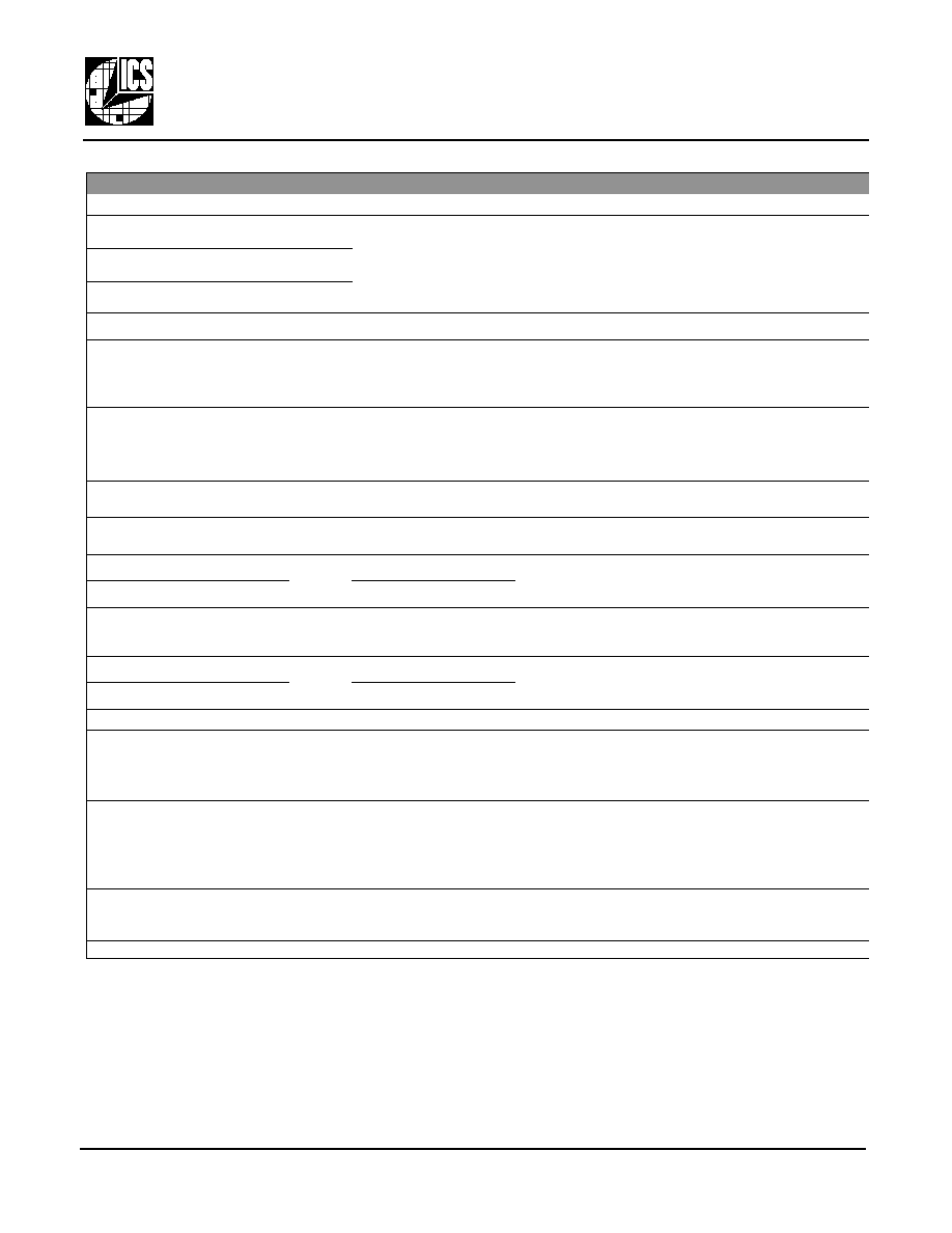
PIN DESCRIPTIONS
Number
Name
I/O
Configuration
Description
1, 2, 3, 10, 14, 26
GND
Ground
Power supply ground connections.
4
9
OP_IN
nOP_IN
Input
External loop filter connections.
See Figure 5, External Loop Filter, on pg. 9.
5
8
nOP_OUT
OP_OUT
Output
6
7
nVC
VC
Input
11, 19, 33
VCC
Power
Power supply connection, connect to +3.3V.
12
AUTO
Input
Internal pull-down resistor1
Automatic/manual reselection mode for clock input:
Logic 1 automatic reselection upon clock failure
(non-revertive)
Logic 0 manual selection only (using REF_SEL)
13
REF_ACK
Output
Reference Acknowledgement pin for input mux state; outputs
the currently selected reference input pair:
Logic 1 indicates nDIF_REF1, DIF_REF1
Logic 0 indicates nDIF_REF0, DIF_REF0
15
16
FOUT
nFOUT
Output
No internal terminator
Clock output pair. Differential LVPECL (CML, LVDS available).
17
18
P_SEL1
P_SEL0
Internal pull-down resistor1
Note 1: For typical values of internal pull-down and pull-UP resistors, see DC Characteristics on pg. 11.
Post-PLL, P divider selection. LVCMOS/LVTTL. See Table 5, P
Divider Look-Up Table (LUT), on pg. 4.
20
nDIF_REF1
Input
Biased to Vcc/2 2
Note 2: Biased to Vcc/2, with 50k
to Vcc and 50k to ground. See Differential Inputs Biased to VCC/2 on pg. 11.
Note 3: See LVCMOS Output in DC Characteristics on pg. 11.
Reference clock input pair 1. Differential LVPECL or LVDS.
Resistor bias on inverting terminal supports TTL or LVCMOS.
21
DIF_REF1
Internal pull-down resistor1
22
REF_SEL
Input
Internal pull-down resistor1
Reference clock input selection. LVCMOS/LVTTL:
Logic 1 selects DIF_REF1, nDIF_REF1.
Logic 0 selects DIF_REF0, nDIF_REF0.
23
nDIF_REF0
Input
Biased to Vcc/2 2
Reference clock input pair 0. Differential LVPECL or LVDS.
Resistor bias on inverting terminal supports TTL or LVCMOS.
24
DIF_REF0
Internal pull-down resistor 1
25
NC
No internal connection
27
28
29
30
MR_SEL3
MR_SEL2
MR_SEL0
MR_SEL1
Input
Internal pull-down resistor1
M and R divider value selection. LVCMOS/ LVTTL.
See Tables 3 and 4, M and R Divider Look-Up Tables (LUT)
on pg. 3.
31
LOR
Output
Loss of Reference indicator. Asserted when there are no clock
edges at the selected input port for 3 clock edges of the PLL
phase detector. 3
Logic 1 indicates loss of reference.
Logic 0 indicates active reference.
32
NBW
Input
Internal pull-UP resistor1
Narrow Bandwidth enable. LVCMOS/LVTTL:
Logic 1 - Narrow loop bandwidth, R
IN = 2100k
.
Logic 0 - Wide bandwidth, R
IN = 100k
.
34, 35, 36
DNC
Do Not Connect.
Table 2: Pin Descriptions
相关PDF资料 |
PDF描述 |
|---|---|
| M210P622.080-023M | SPECIALTY LOGIC CIRCUIT, MDIP24 |
| M210EXXX.XXXX-111K | SPECIALTY LOGIC CIRCUIT, MDIP24 |
| M210EXXX.XXXX-122K | SPECIALTY LOGIC CIRCUIT, MDIP24 |
| M210EXXX.XXXX-130K | SPECIALTY LOGIC CIRCUIT, MDIP24 |
| MDDPGM-TTL-30-30 | PULSE GENERATOR DELAY LINE, TRUE OUTPUT, PDIP4 |
相关代理商/技术参数 |
参数描述 |
|---|---|
| M1034 | 制造商:ICS 制造商全称:ICS 功能描述:VCSO BASED CLOCK PLL WITH AUTOSWITCH |
| M1034-11-155.5200 | 制造商:ICS 制造商全称:ICS 功能描述:VCSO BASED CLOCK PLL WITH AUTOSWITCH |
| M1034-11-156.2500 | 制造商:ICS 制造商全称:ICS 功能描述:VCSO BASED CLOCK PLL WITH AUTOSWITCH |
| M1034-11I155.5200 | 制造商:ICS 制造商全称:ICS 功能描述:VCSO BASED CLOCK PLL WITH AUTOSWITCH |
| M1034-11I156.2500 | 制造商:ICS 制造商全称:ICS 功能描述:VCSO BASED CLOCK PLL WITH AUTOSWITCH |
发布紧急采购,3分钟左右您将得到回复。