参数资料
| 型号: | M1A3P400-1FGG256 |
| 厂商: | Microsemi SoC |
| 文件页数: | 8/12页 |
| 文件大小: | 0K |
| 描述: | IC FPGA 1KB FLASH 400K 256-FBGA |
| 标准包装: | 90 |
| 系列: | ProASIC3 |
| RAM 位总计: | 55296 |
| 输入/输出数: | 178 |
| 门数: | 400000 |
| 电源电压: | 1.425 V ~ 1.575 V |
| 安装类型: | 表面贴装 |
| 工作温度: | 0°C ~ 70°C |
| 封装/外壳: | 256-LBGA |
| 供应商设备封装: | 256-FPBGA(17x17) |
ARM CortexTM-M1
Prod uct Br ief
5
Programmer’s Model
The ARM Cortex-M1 processor supports all ARMv6-M
Thumb instructions. This includes the entire 16-bit
Thumb instruction set architecture and some 32-bit
instructions.
or
information
on
ARMv6-M
Thumb
instructions, see the ARMv6-M Architecture Reference
Manual.
The
processor
does
not
support
ARM
instructions.
Processor Operating States
The ARM Cortex-M1 processor has two operating states:
Thumb state – This is the normal execution state,
with the processor running the 16-bit and 32-bit
halfword-aligned Thumb and Thumb-2 BL, MRS,
MSR, ISB, DSB, and DMB instructions.
Debug state – This is the state the processor is in
for debugging.
Processor Operating Modes
The ARM Cortex-M1 processor supports two modes of
operation:
Thread mode – Entered on Reset, and can be re-
entered as a result of an exception return.
Handler mode – Entered as a result of an
exception.
Main Stack and Process Stack Access
Out of reset, all code uses the main stack. An exception
handler such as SVC can change the stack used by Thread
mode from main stack to process stack by changing the
EXC_RETURN value it uses on exit. All exceptions
continue to use the main stack. The stack pointer, R13, is
a banked register that switches between the main stack
and the process stack. Only one stack, either the process
stack or the main stack, is visible, using R13, at any time.
It is also possible to switch from the main stack to process
stack while in Thread mode by writing to the special
purpose Control Register using an MSR instruction.
Registers
The
processor
has
the
following
32-bit
registers
13 general purpose registers, R0–R12
Stack Pointer (SP) (SP, R13) and banked register
aliases, SP_process and SP_main
Link Register (LR, R14)
Program Counter (PC, R15)
Program status registers (xPSR)
General Purpose Registers
The general purpose registers, R0–R12, have no special
architecturally-defined uses.
Low registers – Registers R0–R7 are accessible by
all instructions that specify a general purpose
register.
High
registers
–
Registers R8-R12 are not
accessible by all 16-bit instructions.
The R13, R14, and R15 registers have the following
special functions:
Stack Pointer – Register R13 is used as the Stack
Pointer (SP). Because the SP ignores writes to bits
[1:0], it is auto-aligned to a word, four-byte, and
boundary. Handler mode always uses SP_main, but
you can configure Thread mode to use either
SP_main or SP_process.
Link Register – Register R14 is the subroutine
Link Register (LR). The LR receives the return
address from PC when a Branch and Link (BL)
instruction is executed. The LR is also used for an
exception return. At all other times, you can treat
R14 as a general purpose register.
Program Counter – Register R15 is the Program
Counter (PC). Bit 0 is always 0, so instructions are
always aligned to halfword boundaries.
Special Purpose Program Status Registers
(xPSR)
Processor status at the system level breaks down into
three categories and can be accessed as individual
registers, a combination of any two from three, or a
combination of all three, using the MRS and MSR
instructions.
Application PSR (APSR) – Contains the condition
code flags. Before entering an exception, the
processor saves the condition code flags on the
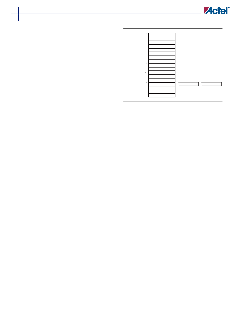
Figure 2 Processor Register Set
r1
r2
r3
r4
r5
r0
High Registers
Low Registers
r9
r10
r11
r12
Program
Status Register
r8
r7
r6
r13 (SP)
r14 (LR)
r15 (PC)
xPSR
SP_main
SP_process
相关PDF资料 |
PDF描述 |
|---|---|
| ASM36DRKF-S13 | CONN EDGECARD 72POS .156 EXTEND |
| AMM36DRKF-S13 | CONN EDGECARD 72POS .156 EXTEND |
| ACM44DSES | CONN EDGECARD 88POS .156 EYELET |
| AT28HC256E-70JU | IC EEPROM 256KBIT 70NS 32PLCC |
| ABM44DSES | CONN EDGECARD 88POS .156 EYELET |
相关代理商/技术参数 |
参数描述 |
|---|---|
| M1A3P400-1FGG256I | 功能描述:IC FPGA 1KB FLASH 400K 256-FBGA RoHS:是 类别:集成电路 (IC) >> 嵌入式 - FPGA(现场可编程门阵列) 系列:ProASIC3 标准包装:90 系列:ProASIC3 LAB/CLB数:- 逻辑元件/单元数:- RAM 位总计:36864 输入/输出数:157 门数:250000 电源电压:1.425 V ~ 1.575 V 安装类型:表面贴装 工作温度:-40°C ~ 125°C 封装/外壳:256-LBGA 供应商设备封装:256-FPBGA(17x17) |
| M1A3P400-1FGG484 | 功能描述:IC FPGA 1KB FLASH 400K 484-FBGA RoHS:是 类别:集成电路 (IC) >> 嵌入式 - FPGA(现场可编程门阵列) 系列:ProASIC3 标准包装:90 系列:ProASIC3 LAB/CLB数:- 逻辑元件/单元数:- RAM 位总计:36864 输入/输出数:157 门数:250000 电源电压:1.425 V ~ 1.575 V 安装类型:表面贴装 工作温度:-40°C ~ 125°C 封装/外壳:256-LBGA 供应商设备封装:256-FPBGA(17x17) |
| M1A3P400-1FGG484I | 功能描述:IC FPGA 1KB FLASH 400K 484-FBGA RoHS:是 类别:集成电路 (IC) >> 嵌入式 - FPGA(现场可编程门阵列) 系列:ProASIC3 标准包装:90 系列:ProASIC3 LAB/CLB数:- 逻辑元件/单元数:- RAM 位总计:36864 输入/输出数:157 门数:250000 电源电压:1.425 V ~ 1.575 V 安装类型:表面贴装 工作温度:-40°C ~ 125°C 封装/外壳:256-LBGA 供应商设备封装:256-FPBGA(17x17) |
| M1A3P400-1PQ144 | 制造商:ACTEL 制造商全称:Actel Corporation 功能描述:ProASIC3 Flash Family FPGAs |
| M1A3P400-1PQ144ES | 制造商:ACTEL 制造商全称:Actel Corporation 功能描述:ProASIC3 Flash Family FPGAs |
发布紧急采购,3分钟左右您将得到回复。