- 您现在的位置:买卖IC网 > PDF目录180063 > M1A3P400-1FGG256II FPGA, 9216 CLBS, 400000 GATES, 350 MHz, PBGA256 PDF资料下载
参数资料
| 型号: | M1A3P400-1FGG256II |
| 元件分类: | FPGA |
| 英文描述: | FPGA, 9216 CLBS, 400000 GATES, 350 MHz, PBGA256 |
| 封装: | 17 X 17 MM, 1.60 MM HEIGHT, 1 MM PITCH, GREEN, FBGA-256 |
| 文件页数: | 49/49页 |
| 文件大小: | 5893K |
| 代理商: | M1A3P400-1FGG256II |
第1页第2页第3页第4页第5页第6页第7页第8页第9页第10页第11页第12页第13页第14页第15页第16页第17页第18页第19页第20页第21页第22页第23页第24页第25页第26页第27页第28页第29页第30页第31页第32页第33页第34页第35页第36页第37页第38页第39页第40页第41页第42页第43页第44页第45页第46页第47页第48页当前第49页
ProASIC3 DC and Switching Characteristics
2- 82
v1.3
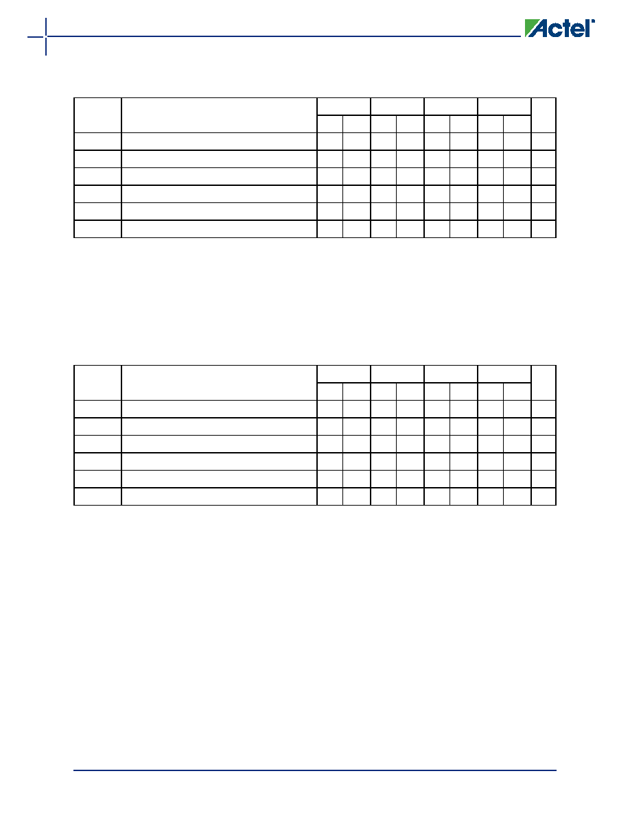
Table 2-104 A3P600 Global Resource
Commercial-Case Conditions: TJ = 70°C, VCC = 1.425 V
Parameter
Description
–2
–1
Std.
–F
Units
Min.1 Max.2 Min.1 Max.2 Min.1 Max.2 Min.1 Max.2
tRCKL
Input LOW Delay for Global Clock
0.87 1.09 0.99 1.24 1.17 1.46 1.40 1.75
ns
tRCKH
Input HIGH Delay for Global Clock
0.861.11 0.981.271.151.491.381.79
ns
tRCKMPWH Minimum Pulse Width HIGH for Global Clock
ns
tRCKMPWL Minimum Pulse Width LOW for Global Clock
ns
tRCKSW
Maximum Skew for Global Clock
0.26
0.29
0.34
0.41
ns
FRMAX
Maximum Frequency for Global Clock
MHz
Notes:
1. Value reflects minimum load. The delay is measured from the CCC output to the clock pin of a sequential
element, located in a lightly loaded row (single element is connected to the global net).
2. Value reflects maximum load. The delay is measured on the clock pin of the farthest sequential element,
located in a fully loaded row (all available flip-flops are connected to the global net in the row).
3. For specific junction temperature and voltage supply levels, refer to Table 2-6 on page 2-6 for derating
values.
Table 2-105 A3P1000 Global Resource
Commercial-Case Conditions: TJ = 70°C, VCC = 1.425 V
Parameter
Description
–2
–1
Std.
–F
Units
Min.1 Max.2 Min.1 Max.2 Min.1 Max.2 Min.1 Max.2
tRCKL
Input LOW Delay for Global Clock
0.94 1.16 1.07 1.32 1.26 1.55 1.51 1.86
ns
tRCKH
Input HIGH Delay for Global Clock
0.931.19 1.061.351.241.591.491.91
ns
tRCKMPWH Minimum Pulse Width HIGH for Global Clock
ns
tRCKMPWL Minimum Pulse Width LOW for Global Clock
ns
tRCKSW
Maximum Skew for Global Clock
0.26
0.29
0.35
0.41
ns
FRMAX
Maximum Frequency for Global Clock
MHz
Notes:
1. Value reflects minimum load. The delay is measured from the CCC output to the clock pin of a sequential
element, located in a lightly loaded row (single element is connected to the global net).
2. Value reflects maximum load. The delay is measured on the clock pin of the farthest sequential element,
located in a fully loaded row (all available flip-flops are connected to the global net in the row).
3. For specific junction temperature and voltage supply levels, refer to Table 2-6 on page 2-6 for derating
values.
相关PDF资料 |
PDF描述 |
|---|---|
| M1A3P400-1FGG484II | FPGA, 9216 CLBS, 400000 GATES, 350 MHz, PBGA484 |
| M1A3P400-1PQ208II | FPGA, 9216 CLBS, 400000 GATES, 350 MHz, PQFP208 |
| M1A3P400-1PQG208II | FPGA, 9216 CLBS, 400000 GATES, 350 MHz, PQFP208 |
| M1A3P400-2FG144II | FPGA, 9216 CLBS, 400000 GATES, 350 MHz, PBGA144 |
| M1A3P400-2FG256II | FPGA, 9216 CLBS, 400000 GATES, 350 MHz, PBGA256 |
相关代理商/技术参数 |
参数描述 |
|---|---|
| M1A3P400-1FGG484 | 功能描述:IC FPGA 1KB FLASH 400K 484-FBGA RoHS:是 类别:集成电路 (IC) >> 嵌入式 - FPGA(现场可编程门阵列) 系列:ProASIC3 标准包装:90 系列:ProASIC3 LAB/CLB数:- 逻辑元件/单元数:- RAM 位总计:36864 输入/输出数:157 门数:250000 电源电压:1.425 V ~ 1.575 V 安装类型:表面贴装 工作温度:-40°C ~ 125°C 封装/外壳:256-LBGA 供应商设备封装:256-FPBGA(17x17) |
| M1A3P400-1FGG484I | 功能描述:IC FPGA 1KB FLASH 400K 484-FBGA RoHS:是 类别:集成电路 (IC) >> 嵌入式 - FPGA(现场可编程门阵列) 系列:ProASIC3 标准包装:90 系列:ProASIC3 LAB/CLB数:- 逻辑元件/单元数:- RAM 位总计:36864 输入/输出数:157 门数:250000 电源电压:1.425 V ~ 1.575 V 安装类型:表面贴装 工作温度:-40°C ~ 125°C 封装/外壳:256-LBGA 供应商设备封装:256-FPBGA(17x17) |
| M1A3P400-1PQ144 | 制造商:ACTEL 制造商全称:Actel Corporation 功能描述:ProASIC3 Flash Family FPGAs |
| M1A3P400-1PQ144ES | 制造商:ACTEL 制造商全称:Actel Corporation 功能描述:ProASIC3 Flash Family FPGAs |
| M1A3P400-1PQ144I | 制造商:ACTEL 制造商全称:Actel Corporation 功能描述:ProASIC3 Flash Family FPGAs |
发布紧急采购,3分钟左右您将得到回复。