参数资料
| 型号: | M1A3P600-FGG144 |
| 厂商: | Microsemi SoC |
| 文件页数: | 9/12页 |
| 文件大小: | 0K |
| 描述: | IC FPGA 1KB FLASH 600K 144-FBGA |
| 标准包装: | 160 |
| 系列: | ProASIC3 |
| RAM 位总计: | 110592 |
| 输入/输出数: | 97 |
| 门数: | 600000 |
| 电源电压: | 1.425 V ~ 1.575 V |
| 安装类型: | 表面贴装 |
| 工作温度: | 0°C ~ 70°C |
| 封装/外壳: | 144-LBGA |
| 供应商设备封装: | 144-FPBGA(13x13) |
ARM CortexTM-M1
6P ro d u c t B r i e f
stack. You can access the APSR with the MSR and
MRS instructions.
Interrupt PSR (IPSR) – Contains the Interrupt
Service Routine (ISR) number of the current
exception activation.
Execution PSR (EPSR) – Contains the Thumb state
bit (T-bit). Unless the processor is in Debug state,
the EPSR is not directly accessible. All fields read as
zero using an MRS instruction and MSR instruction
writes are ignored.
On entering an exception, the processor saves the
combined information from the three status registers on
the stack.
Special Purpose Priority Mask Register
Use the special purpose Priority Mask Register for
priority boosting. You can access the special purpose
Priority
Mask
Register
using
the
MSR
and
MRS
instructions. You can also use the CPS instruction to set or
clear PRIMASK.
Special Purpose Control Register
The special purpose Control Register identifies the stack
pointers used.
Data Types
The processor supports the following data types:
32-bit words
16-bit halfwords
8-bit bytes
Note: Unless otherwise stated, the core can access all
regions of the memory map, including the code region,
with all data types. To support this, the system must
support sub-word writes without corrupting neighboring
bytes in that word.
Memory Formats
The processor views memory as a linear collection of
bytes numbered in ascending order from 0 (Figure 3).
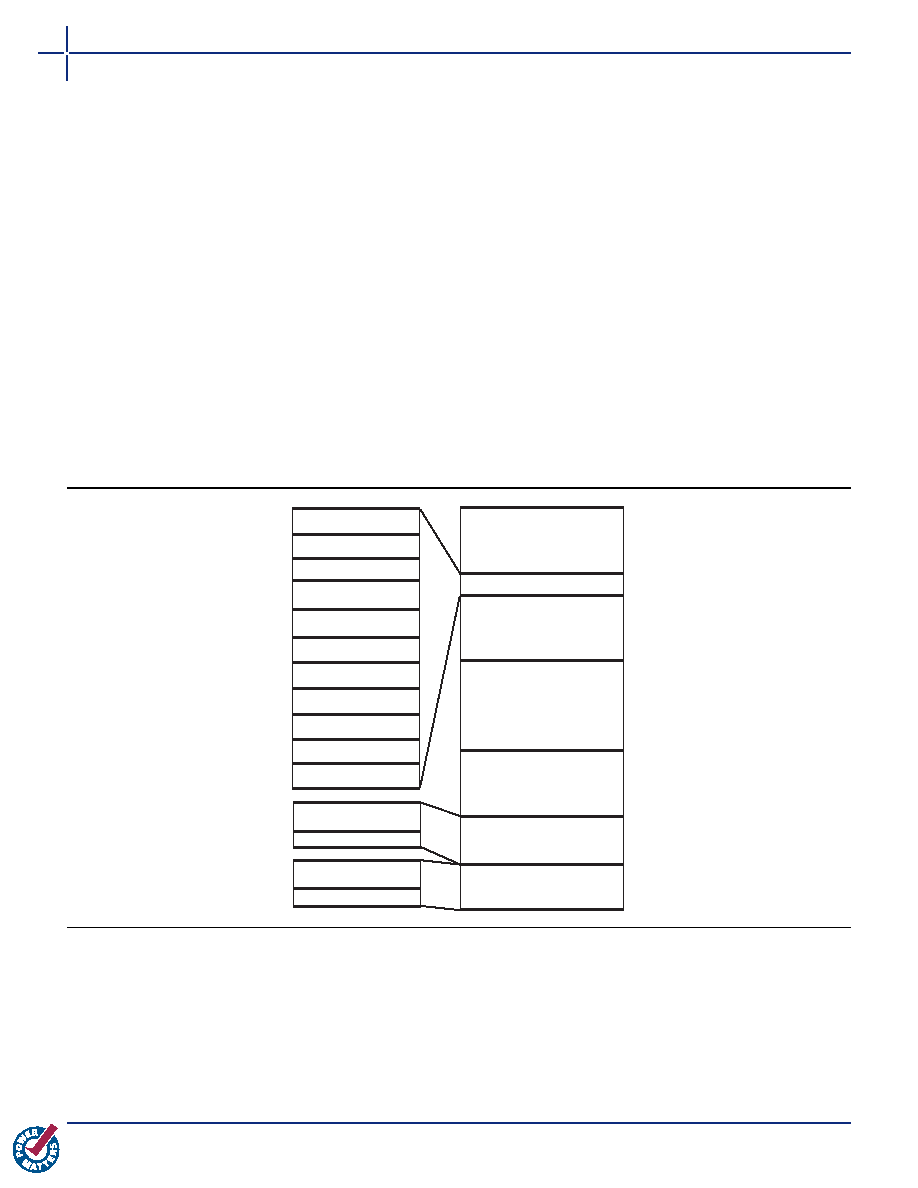
Figure 3 Processor Memory Map
0xE00FFFFF
0xF00FF000
0xE000ED00
0xE000E000
0xE0003000
0xE0002000
0xE0001000
0xE0000000
0xE000F000
0xE003FFFF
0xE0040000
0xE0041000
0xE0042000
ROM Table
Reserved
BP
DW
Reserved
NVIC
Debug Control
Reserved
0x3FFFFFFF
0x20100000
511 MB
1 MB
511 MB
1 MB
External
DTCM
External
ITCM
0x00100000
0x1FFFFFFF
0x20000000
0x00000000
Reserved
Internal Private Peripheral Bus
1 GB
0.5 GB
Code
SRAM
Peripheral
External
External Device
0.5 GB
0xFFFFFFFF
0xE0100000
0x5FFFFFFF
0x40000000
0x3FFFFFFF
0x20000000
0x1FFFFFFF
0x00000000
0x60000000
0x9FFFFFFF
0xA0000000
0xDFFFFFFF
0x00000000
相关PDF资料 |
PDF描述 |
|---|---|
| A3P600-FG144 | IC FPGA 1KB FLASH 600K 144-FBGA |
| M1A3P600-FG144 | IC FPGA 1KB FLASH 600K 144-FBGA |
| EX256-TQ100A | IC FPGA ANTIFUSE 12K 100-TQFP |
| EX256-TQG100A | IC FPGA ANTIFUSE 12K 100-TQFP |
| EP4CE10E22I8L | IC CYCLONE IV FPGA 10K 144EQFP |
相关代理商/技术参数 |
参数描述 |
|---|---|
| M1A3P600-FGG144ES | 制造商:ACTEL 制造商全称:Actel Corporation 功能描述:ProASIC3 Flash Family FPGAs |
| M1A3P600-FGG144I | 功能描述:IC FPGA 1KB FLASH 600K 144-FBGA RoHS:是 类别:集成电路 (IC) >> 嵌入式 - FPGA(现场可编程门阵列) 系列:ProASIC3 标准包装:90 系列:ProASIC3 LAB/CLB数:- 逻辑元件/单元数:- RAM 位总计:36864 输入/输出数:157 门数:250000 电源电压:1.425 V ~ 1.575 V 安装类型:表面贴装 工作温度:-40°C ~ 125°C 封装/外壳:256-LBGA 供应商设备封装:256-FPBGA(17x17) |
| M1A3P600-FGG144PP | 制造商:ACTEL 制造商全称:Actel Corporation 功能描述:ProASIC3 Flash Family FPGAs |
| M1A3P600-FGG256 | 功能描述:IC FPGA 1KB FLASH 600K 256-FBGA RoHS:是 类别:集成电路 (IC) >> 嵌入式 - FPGA(现场可编程门阵列) 系列:ProASIC3 标准包装:90 系列:ProASIC3 LAB/CLB数:- 逻辑元件/单元数:- RAM 位总计:36864 输入/输出数:157 门数:250000 电源电压:1.425 V ~ 1.575 V 安装类型:表面贴装 工作温度:-40°C ~ 125°C 封装/外壳:256-LBGA 供应商设备封装:256-FPBGA(17x17) |
| M1A3P600-FGG256I | 功能描述:IC FPGA 1KB FLASH 600K 256-FBGA RoHS:是 类别:集成电路 (IC) >> 嵌入式 - FPGA(现场可编程门阵列) 系列:ProASIC3 标准包装:90 系列:ProASIC3 LAB/CLB数:- 逻辑元件/单元数:- RAM 位总计:36864 输入/输出数:157 门数:250000 电源电压:1.425 V ~ 1.575 V 安装类型:表面贴装 工作温度:-40°C ~ 125°C 封装/外壳:256-LBGA 供应商设备封装:256-FPBGA(17x17) |
发布紧急采购,3分钟左右您将得到回复。