参数资料
| 型号: | M1A3PE3000-1FGG484I |
| 厂商: | Microsemi SoC |
| 文件页数: | 122/162页 |
| 文件大小: | 0K |
| 描述: | IC FPGA 1KB FLASH 3M 484-FBGA |
| 标准包装: | 40 |
| 系列: | ProASIC3E |
| RAM 位总计: | 516096 |
| 输入/输出数: | 341 |
| 门数: | 3000000 |
| 电源电压: | 1.425 V ~ 1.575 V |
| 安装类型: | 表面贴装 |
| 工作温度: | -40°C ~ 85°C |
| 封装/外壳: | 484-BGA |
| 供应商设备封装: | 484-FPBGA(23x23) |
第1页第2页第3页第4页第5页第6页第7页第8页第9页第10页第11页第12页第13页第14页第15页第16页第17页第18页第19页第20页第21页第22页第23页第24页第25页第26页第27页第28页第29页第30页第31页第32页第33页第34页第35页第36页第37页第38页第39页第40页第41页第42页第43页第44页第45页第46页第47页第48页第49页第50页第51页第52页第53页第54页第55页第56页第57页第58页第59页第60页第61页第62页第63页第64页第65页第66页第67页第68页第69页第70页第71页第72页第73页第74页第75页第76页第77页第78页第79页第80页第81页第82页第83页第84页第85页第86页第87页第88页第89页第90页第91页第92页第93页第94页第95页第96页第97页第98页第99页第100页第101页第102页第103页第104页第105页第106页第107页第108页第109页第110页第111页第112页第113页第114页第115页第116页第117页第118页第119页第120页第121页当前第122页第123页第124页第125页第126页第127页第128页第129页第130页第131页第132页第133页第134页第135页第136页第137页第138页第139页第140页第141页第142页第143页第144页第145页第146页第147页第148页第149页第150页第151页第152页第153页第154页第155页第156页第157页第158页第159页第160页第161页第162页
ProASIC3E DC and Switching Characteristics
2-48
Revision 13
Differential I/O Characteristics
Physical Implementation
Configuration of the I/O modules as a differential pair is handled by the Designer software when the user
instantiates a differential I/O macro in the design.
Differential I/Os can also be used in conjunction with the embedded Input Register (InReg), Output
Register (OutReg), Enable Register (EnReg), and DDR. However, there is no support for bidirectional
I/Os or tristates with the LVPECL standards.
LVDS
Low-Voltage Differential Signaling (ANSI/TIA/EIA-644) is a high-speed, differential I/O standard. It
requires that one data bit be carried through two signal lines, so two pins are needed. It also requires
external resistor termination.
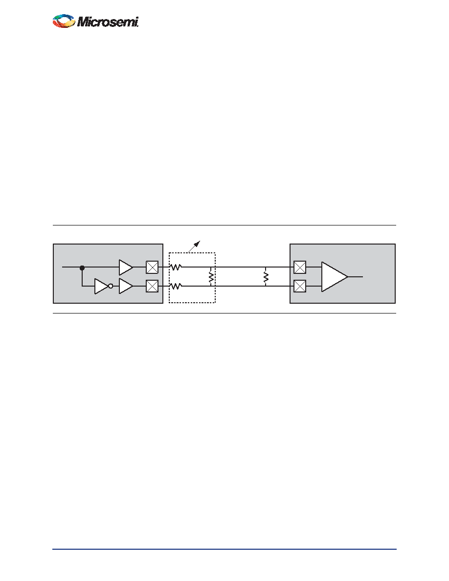
The full implementation of the LVDS transmitter and receiver is shown in an example in Figure 2-22. The
building blocks of the LVDS transmitter-receiver are one transmitter macro, one receiver macro, three
board resistors at the transmitter end, and one resistor at the receiver end. The values for the three driver
resistors are different from those used in the LVPECL implementation because the output standard
specifications are different.
Along with LVDS I/O, ProASIC3E also supports Bus LVDS structure and Multipoint LVDS (M-LVDS)
configuration (up to 40 nodes).
Figure 2-22 LVDS Circuit Diagram and Board-Level Implementation
140
100
Z0 = 50
165
165
+
–
P
N
P
N
INBUF_LVDS
OUTBUF_LVDS
FPGA
Bourns Part Number: CAT16-LV4F12
相关PDF资料 |
PDF描述 |
|---|---|
| IDT70V3599S133BCI | IC SRAM 4MBIT 133MHZ 256BGA |
| A3PE3000-1FG484I | IC FPGA 1KB FLASH 3M 484-FBGA |
| A3PE3000-1FGG484I | IC FPGA 1KB FLASH 3M 484-FBGA |
| EP1S20F780C6N | IC STRATIX FPGA 20K LE 780-FBGA |
| A1240A-1PQG144C | IC FPGA 4K GATES 144-PQFP COM |
相关代理商/技术参数 |
参数描述 |
|---|---|
| M1A3PE3000-1FGG896 | 功能描述:IC FPGA 1KB FLASH 3M 896-FBGA RoHS:是 类别:集成电路 (IC) >> 嵌入式 - FPGA(现场可编程门阵列) 系列:ProASIC3E 产品培训模块:Three Reasons to Use FPGA's in Industrial Designs Cyclone IV FPGA Family Overview 特色产品:Cyclone? IV FPGAs 标准包装:60 系列:CYCLONE® IV GX LAB/CLB数:9360 逻辑元件/单元数:149760 RAM 位总计:6635520 输入/输出数:270 门数:- 电源电压:1.16 V ~ 1.24 V 安装类型:表面贴装 工作温度:0°C ~ 85°C 封装/外壳:484-BGA 供应商设备封装:484-FBGA(23x23) |
| M1A3PE3000-1FGG896ES | 制造商:ACTEL 制造商全称:Actel Corporation 功能描述:ProASIC3E Flash Family FPGAs |
| M1A3PE3000-1FGG896I | 功能描述:IC FPGA 1KB FLASH 3M 896-FBGA RoHS:是 类别:集成电路 (IC) >> 嵌入式 - FPGA(现场可编程门阵列) 系列:ProASIC3E 标准包装:1 系列:ProASICPLUS LAB/CLB数:- 逻辑元件/单元数:- RAM 位总计:129024 输入/输出数:248 门数:600000 电源电压:2.3 V ~ 2.7 V 安装类型:表面贴装 工作温度:- 封装/外壳:352-BFCQFP,带拉杆 供应商设备封装:352-CQFP(75x75) |
| M1A3PE3000-1FGG896PP | 制造商:ACTEL 制造商全称:Actel Corporation 功能描述:ProASIC3E Flash Family FPGAs |
| M1A3PE3000-1PQ208 | 功能描述:IC FPGA 1KB FLASH 3M 208-PQFP RoHS:否 类别:集成电路 (IC) >> 嵌入式 - FPGA(现场可编程门阵列) 系列:ProASIC3E 产品培训模块:Three Reasons to Use FPGA's in Industrial Designs Cyclone IV FPGA Family Overview 特色产品:Cyclone? IV FPGAs 标准包装:60 系列:CYCLONE® IV GX LAB/CLB数:9360 逻辑元件/单元数:149760 RAM 位总计:6635520 输入/输出数:270 门数:- 电源电压:1.16 V ~ 1.24 V 安装类型:表面贴装 工作温度:0°C ~ 85°C 封装/外壳:484-BGA 供应商设备封装:484-FBGA(23x23) |
发布紧急采购,3分钟左右您将得到回复。