- 您现在的位置:买卖IC网 > PDF目录95857 > M1MA141KT3 (MOTOROLA INC) SILICON, SIGNAL DIODE PDF资料下载
参数资料
| 型号: | M1MA141KT3 |
| 厂商: | MOTOROLA INC |
| 元件分类: | 二极管(射频、小信号、开关、功率) |
| 英文描述: | SILICON, SIGNAL DIODE |
| 文件页数: | 4/6页 |
| 文件大小: | 95K |
| 代理商: | M1MA141KT3 |
M1MA141KT1 M1MA142KT1
4
Motorola Small–Signal Transistors, FETs and Diodes Device Data
SOLDER STENCIL GUIDELINES
Prior to placing surface mount components onto a printed
circuit board, solder paste must be applied to the pads. A
solder stencil is required to screen the optimum amount of
solder paste onto the footprint. The stencil is made of brass
or stainless steel with a typical thickness of 0.008 inches.
The stencil opening size for the surface mounted package
should be the same as the pad size on the printed circuit
board, i.e., a 1:1 registration.
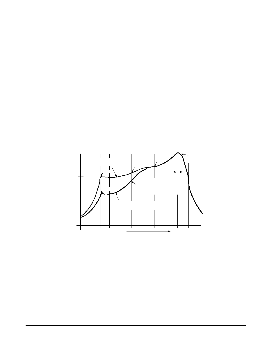
TYPICAL SOLDER HEATING PROFILE
For any given circuit board, there will be a group of control
settings that will give the desired heat pattern. The operator
must set temperatures for several heating zones, and a
figure for belt speed. Taken together, these control settings
make up a heating “profile” for that particular circuit board.
On machines controlled by a computer, the computer
remembers these profiles from one operating session to the
next. Figure 4 shows a typical heating profile for use when
soldering a surface mount device to a printed circuit board.
This profile will vary among soldering systems but it is a good
starting point. Factors that can affect the profile include the
type of soldering system in use, density and types of
components on the board, type of solder used, and the type
of board or substrate material being used. This profile shows
temperature versus time. The line on the graph shows the
actual temperature that might be experienced on the surface
of a test board at or near a central solder joint. The two
profiles are based on a high density and a low density board.
The Vitronics SMD310 convection/infrared reflow soldering
system was used to generate this profile. The type of solder
used was 62/36/2 Tin Lead Silver with a melting point
between 177 –189
°C. When this type of furnace is used for
solder reflow work, the circuit boards and solder joints tend to
heat first. The components on the board are then heated by
conduction. The circuit board, because it has a large surface
area, absorbs the thermal energy more efficiently, then
distributes this energy to the components. Because of this
effect, the main body of a component may be up to 30
degrees cooler than the adjacent solder joints.
STEP 1
PREHEAT
ZONE 1
“RAMP”
STEP 2
VENT
“SOAK”
STEP 3
HEATING
ZONES 2 & 5
“RAMP”
STEP 4
HEATING
ZONES 3 & 6
“SOAK”
STEP 5
HEATING
ZONES 4 & 7
“SPIKE”
STEP 6
VENT
STEP 7
COOLING
200
°C
150
°C
100
°C
50
°C
TIME (3 TO 7 MINUTES TOTAL)
TMAX
SOLDER IS LIQUID FOR
40 TO 80 SECONDS
(DEPENDING ON
MASS OF ASSEMBLY)
205
° TO 219°C
PEAK AT
SOLDER JOINT
DESIRED CURVE FOR LOW
MASS ASSEMBLIES
100
°C
150
°C
160
°C
140
°C
Figure 4. Typical Solder Heating Profile
DESIRED CURVE FOR HIGH
MASS ASSEMBLIES
170
°C
相关PDF资料 |
PDF描述 |
|---|---|
| M1MA141WKT3 | 0.1 A, 2 ELEMENT, SILICON, SIGNAL DIODE |
| M1MA151WAT3 | 0.1 A, 40 V, 2 ELEMENT, SILICON, SIGNAL DIODE |
| M1MA152/2AT3 | 0.1 A, 80 V, SILICON, SIGNAL DIODE |
| M1MA152/2AT1 | 0.1 A, 40 V, SILICON, SIGNAL DIODE |
| M1MA152AT3 | 0.1 A, 80 V, SILICON, SIGNAL DIODE |
相关代理商/技术参数 |
参数描述 |
|---|---|
| M1MA141WA | 制造商:LUGUANG 制造商全称:Shenzhen Luguang Electronic Technology Co., Ltd 功能描述:Surface Mount Switching Diodes |
| M1MA141WAT1 | 功能描述:二极管 - 通用,功率,开关 40V 100mA RoHS:否 制造商:STMicroelectronics 产品:Switching Diodes 峰值反向电压:600 V 正向连续电流:200 A 最大浪涌电流:800 A 配置: 恢复时间:2000 ns 正向电压下降:1.25 V 最大反向漏泄电流:300 uA 最大功率耗散: 工作温度范围: 安装风格:SMD/SMT 封装 / 箱体:ISOTOP 封装:Tube |
| M1MA141WAT1_05 | 制造商:ONSEMI 制造商全称:ON Semiconductor 功能描述:Common Anode Silicon Dual Switching Diode |
| M1MA141WAT1G | 功能描述:二极管 - 通用,功率,开关 40V 100mA RoHS:否 制造商:STMicroelectronics 产品:Switching Diodes 峰值反向电压:600 V 正向连续电流:200 A 最大浪涌电流:800 A 配置: 恢复时间:2000 ns 正向电压下降:1.25 V 最大反向漏泄电流:300 uA 最大功率耗散: 工作温度范围: 安装风格:SMD/SMT 封装 / 箱体:ISOTOP 封装:Tube |
| M1MA141WK | 制造商:ONSEMI 制造商全称:ON Semiconductor 功能描述:COMMON CATHODE DUAL SWITCHING DIODE |
发布紧急采购,3分钟左右您将得到回复。