- 您现在的位置:买卖IC网 > PDF目录359008 > M28C17-120MS6T (意法半导体) 16K 2K x 8 PARALLEL EEPROM with SOFTWARE DATA PROTECTION PDF资料下载
参数资料
| 型号: | M28C17-120MS6T |
| 厂商: | 意法半导体 |
| 元件分类: | DRAM |
| 英文描述: | 16K 2K x 8 PARALLEL EEPROM with SOFTWARE DATA PROTECTION |
| 中文描述: | 16K的2K × 8的并行EEPROM,带有软件数据保护 |
| 文件页数: | 3/17页 |
| 文件大小: | 165K |
| 代理商: | M28C17-120MS6T |
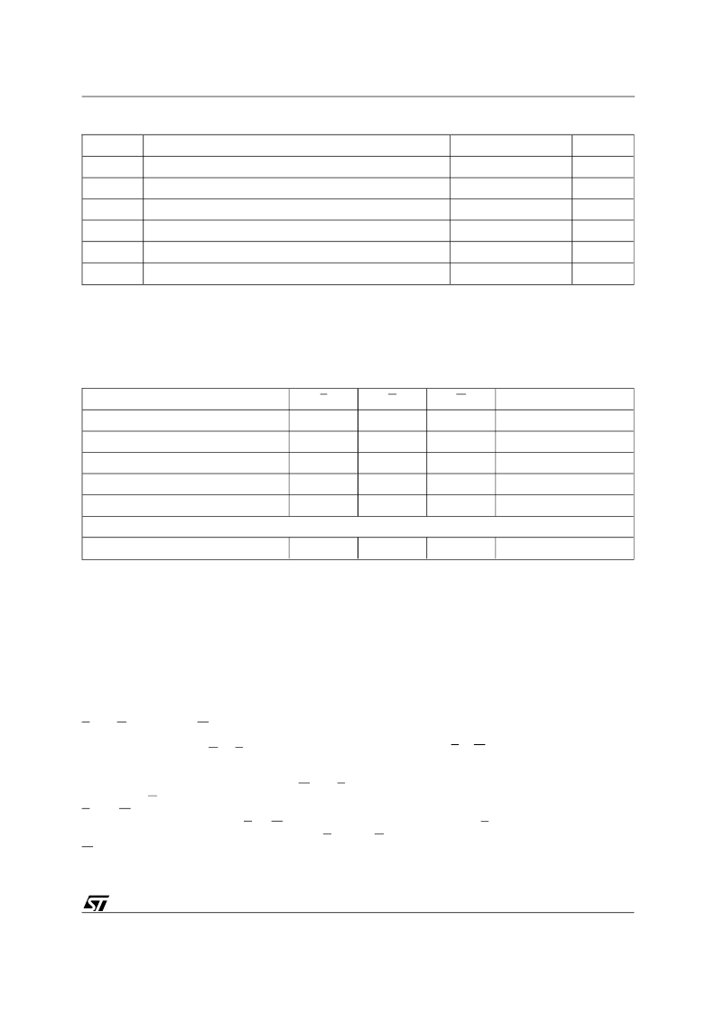
Symbol
Parameter
Value
Unit
T
A
Ambient Operating Temperature
– 40 to 125
°
C
T
STG
Storage Temperature Range
– 65 to 150
°
C
V
CC
Supply Voltage
– 0.3 to 6.5
V
V
IO
Input/Output Voltage
– 0.3 to V
CC
+0.6
V
V
I
Input Voltage
– 0.3 to 6.5
V
V
ESD
Electrostatic Discharge Voltage (Human Body model)
(2)
4000
V
Note:
1. Except for the rating "Operating Temperature Range", stresses above those listed in the Table "Absolute Maximum Ratings" may
cause permanent damage to the device. These are stress ratings only and operation of the device at these or any other conditions
above those indicated in the Operating sections of this specification is not implied. Exposure to Absolute Maximum Rating
conditions for extended periods may affect device reliability. Refer also to the SGS-THOMSON SURE Program and other
relevant quality documents.
2. 100pF through 1500
; MIL-STD-883C, 3015.7
Table 2. Absolute Maximum Ratings
(1)
Mode
E
G
W
DQ0 - DQ7
Standby
1
X
X
Hi-Z
Output Disable
X
1
X
Hi-Z
Write Disable
X
X
1
Hi-Z
Read
0
0
1
Data Out
Write
0
1
0
Data In
Chip Erase
0
V
0
Hi-Z
Note:
1.
0 = V
IL
; 1 = V
IH
; X = V
IL
or V
IH;
V = 12
±
5%.
Table 3. Operating Modes
(1)
OPERATION
In order to prevent data corruption and inadvertent
write operations an internal V
CC
comparator inhibits
Write operation if V
CC
is below V
WI
(see Table 7).
Access to the memory in write mode is allowed after
a power-up as specified in Table 7.
Read
The M28C17 is accessed like a static RAM. When
E and G are low with W high, the data addressed
is presented on the I/O pins. The I/O pins are high
impedance when either G or E is high.
Write
Write operations are initiated when both W and E
are low and G is high.The M28C17 supports both
E and W controlled write cycles. The Address is
latched by the falling edge of E or W which ever
occurs last and the Data on the rising edge of E or
W which ever occurs first. Once initiated the write
operation is internally timed until completion.
Page Write
Page write allows up to 64 bytes to be consecu-
tively latched into the memory prior to initiating a
programming cycle. All bytes must be located in a
single page address, that is A6-A10 must be the
same for all bytes. The page write can be initiated
during any byte write operation.
Following the first byte write instruction the host
may send another address and data with a mini-
mum data transfer rate of 1/t
WHWH
(see Figure 13).
If a transition of E or W is not detected within t
WHWH
,
the internal programming cycle will start.
Chip Erase
The contents of the entire memory may be erased
to FFh by use of the Chip Erase command by
setting Chip Enable (E) Low and Output Enable
(G) to V
CC
+ 7.0V. The chip is cleared when a 10ms
low pulse is applied to the Write Enable pin.
3/17
M28C17
相关PDF资料 |
PDF描述 |
|---|---|
| M28C17-120P1T | 16K 2K x 8 PARALLEL EEPROM with SOFTWARE DATA PROTECTION |
| M28C17-120P6T | 16K 2K x 8 PARALLEL EEPROM with SOFTWARE DATA PROTECTION |
| M28C17-150K1T | CAP 330UF 10V ELECT MZA SMD |
| M28C17-150K6T | 16K 2K x 8 PARALLEL EEPROM with SOFTWARE DATA PROTECTION |
| M28C17-150MS1T | 16K 2K x 8 PARALLEL EEPROM with SOFTWARE DATA PROTECTION |
相关代理商/技术参数 |
参数描述 |
|---|---|
| M28C17-120P1T | 制造商:STMICROELECTRONICS 制造商全称:STMicroelectronics 功能描述:16K 2K x 8 PARALLEL EEPROM with SOFTWARE DATA PROTECTION |
| M28C17-120P6T | 制造商:STMICROELECTRONICS 制造商全称:STMicroelectronics 功能描述:16K 2K x 8 PARALLEL EEPROM with SOFTWARE DATA PROTECTION |
| M28C17-120WK1TR | 制造商:STMICROELECTRONICS 制造商全称:STMicroelectronics 功能描述:16 Kbit 2K x 8 Parallel EEPROM With Software Data Protection |
| M28C17-120WK6TR | 制造商:STMICROELECTRONICS 制造商全称:STMicroelectronics 功能描述:16 Kbit 2K x 8 Parallel EEPROM With Software Data Protection |
| M28C17-150K1T | 制造商:STMICROELECTRONICS 制造商全称:STMicroelectronics 功能描述:16K 2K x 8 PARALLEL EEPROM with SOFTWARE DATA PROTECTION |
发布紧急采购,3分钟左右您将得到回复。