- 您现在的位置:买卖IC网 > PDF目录359010 > M28F101-100P3 (意法半导体) 1 Mb 128K x 8, Chip Erase FLASH MEMORY PDF资料下载
参数资料
| 型号: | M28F101-100P3 |
| 厂商: | 意法半导体 |
| 英文描述: | 1 Mb 128K x 8, Chip Erase FLASH MEMORY |
| 中文描述: | 1 MB的128K的× 8,芯片擦除闪存 |
| 文件页数: | 3/23页 |
| 文件大小: | 197K |
| 代理商: | M28F101-100P3 |
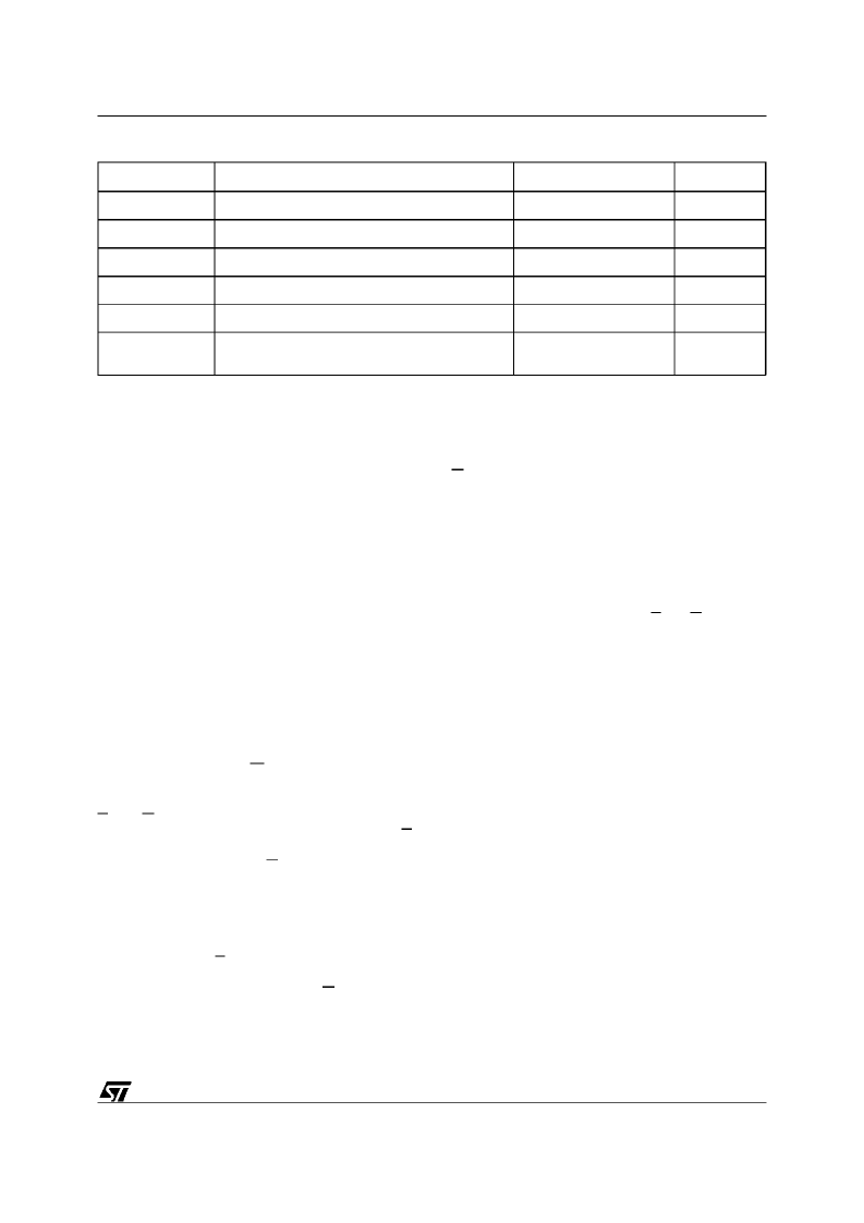
Symbol
Parameter
Value
Unit
T
A
Ambient Operating Temperature
–40 to 125
°
C
T
STG
Storage Temperature
–65 to 150
°
C
V
IO
Input or Output Voltages
–0.6 to 7
V
V
CC
Supply Voltage
–0.6 to 7
V
V
A9
A9 Voltage
–0.6 to 13.5
V
V
PP
Program Supply Voltage, during Erase
or Programming
–0.6 to 14
V
Note:
Except for the rating ”Operating Temperature Range”, stressesabove those listed in the Table ”Absolute Maximum Ratings” may
cause permanent damage to the device. These are stress ratings only and operation ofthe device at these or any other conditions above
those indicated in the Operating sections of this specification is notimplied. Exposure to AbsoluteMaximum Ratingconditions for extended
periods may affect device reliability.Refer also to the SGS-THOMSON SURE Program and other relevant quality documents.
Table 2. Absolute MaximumRatings
DEVICE OPERATION
The M28F101 FLASH Memory employs atechnol-
ogy similar to a 1 MegabitEPROM but addsto the
device functionalityby providingelectrical erasure
and programming. These functions are managed
by a command register. The functions that are
addressed via the command register depend on
the voltage applied to the V
PP
, program voltage,
input. When V
PP
is less than or equal to 6.5V, the
command registeris disabled and M28F101func-
tions as a read only memory providing operating
modes similar to an EPROM (Read, Output Dis-
able, Electronic Signature Read and Standby).
When V
PP
is raised to 12V the command regsiter
is enabledandthisprovides,inaddition,Eraseand
Programoperations.
READONLY MODES, V
PP
≤
6.5V
For all Read Only Modes, except Standby Mode,
the Write Enable input W should be High. In the
StandbyMode this input is don’t care.
Read Mode
. TheM28F101 has two enable inputs,
E and G, both of which must be Low in order to
output datafrom thememory. The ChipEnable(E)
is the power control and shouldbe used for device
selection. Output Enable (G) is the output control
and should be used to gate data on to the output,
independantof the device selection.
Standby Mode.
In the Standby Mode the maxi-
mum supply current is reduced. The device is
placed in the StandbyMode by applyinga Highto
the Chip Enable (E) input. When in the Standby
Mode the outputs are in a high impedance state,
independantof the Output Enable (G) input.
Output Disable Mode
. When the Output Enable
(G) is High the outputs are in a high impedance
state.
ElectronicSignatureMode.
Thismodeallowsthe
read outof two binary codesfrom thedevicewhich
identify the manufacturer and device type. This
mode is intended for use by programmingequip-
ment to automaticallyselect the correct erase and
programmingalgorithms.The ElectronicSignature
Mode is activewhen a high voltage (11.5V to 13V)
isappliedtoaddresslineA9with EandGLow.With
A0 Low the output data is the manufacturercode,
whenA0 isHigh the outputis thedevicetype code.
All other address lines should be maintainedLow
while reading the codes. The electronic signature
may also be accessed in Read/Write modes.
READ/WRITE MODES, 11.4V
≤
V
PP
≤
12.6V
When V
PP
is High both read and write operations
may be performed.These are defined by the con-
tents of an internal command register. Commands
may be written to this register to set-up and exe-
cute,Erase,Erase Verify,Program,ProgramVerify
and Reset modes. Each of these modes needs 2
cycles. Eah mode starts with a write operation to
set-upthe command,thisis followedbyeitherread
or write operations. The device expects the first
cycle to be a write operation and does not corrupt
data at any location in the memory. Read mode is
set-upwith one cycle only and may be followed by
any number of read operations to output data.
ElectronicSignatureReadmodeis set-up with one
cycle and followed by a read cycle to output the
manufactureror devicecodes.
3/23
M28F101
相关PDF资料 |
PDF描述 |
|---|---|
| M28F101-100P1 | 1 Mb 128K x 8, Chip Erase FLASH MEMORY |
| M28F101-100N6 | 1 Mb 128K x 8, Chip Erase FLASH MEMORY |
| M28F101-100N3 | 1 Mb 128K x 8, Chip Erase FLASH MEMORY |
| M28F101-200XP1 | Fuses, 2A 250V SB 5X15 BULK |
| M28F101-150XP1 | FUSE 1A 125V LI |
相关代理商/技术参数 |
参数描述 |
|---|---|
| M28F101-100P6 | 制造商:STMICROELECTRONICS 制造商全称:STMicroelectronics 功能描述:1 Mb 128K x 8, Chip Erase FLASH MEMORY |
| M28F101-100XK1 | 制造商:STMICROELECTRONICS 制造商全称:STMicroelectronics 功能描述:1 Mb 128K x 8, Chip Erase FLASH MEMORY |
| M28F101-100XK3 | 制造商:STMICROELECTRONICS 制造商全称:STMicroelectronics 功能描述:1 Mb 128K x 8, Chip Erase FLASH MEMORY |
| M28F101-100XK6 | 制造商:STMICROELECTRONICS 制造商全称:STMicroelectronics 功能描述:1 Mb 128K x 8, Chip Erase FLASH MEMORY |
| M28F101-100XN1 | 制造商:STMICROELECTRONICS 制造商全称:STMicroelectronics 功能描述:1 Mb 128K x 8, Chip Erase FLASH MEMORY |
发布紧急采购,3分钟左右您将得到回复。