- 您现在的位置:买卖IC网 > PDF目录359010 > M28F101-70N6 (意法半导体) 1 Mb 128K x 8, Chip Erase FLASH MEMORY PDF资料下载
参数资料
| 型号: | M28F101-70N6 |
| 厂商: | 意法半导体 |
| 英文描述: | 1 Mb 128K x 8, Chip Erase FLASH MEMORY |
| 中文描述: | 1 MB的128K的× 8,芯片擦除闪存 |
| 文件页数: | 11/23页 |
| 文件大小: | 197K |
| 代理商: | M28F101-70N6 |
Symbol
Alt
Parameter
M28F101
-90
V
CC
=5V
±
10%
EPROM
Interface
Min
1
1
90
Unit
-70
-100
V
CC
=5V
±
5%
SRAM
Interface
Min
1
1
70
V
CC
=5V
±
10%
EPROM
Interface
Min
1
1
100
Max
Max
Max
t
VPHEL
t
VPHWL
t
WHWH3
t
AVWL
t
AVEL
t
WLAX
t
ELAX
t
ELWL
t
WLEL
V
PP
High to Chip Enable Low
V
PP
High to Write Enable Low
Write Cycle Time
μ
s
μ
s
ns
t
WC
t
AS
Address Validto Write Enable Low
Address Validto Chip Enable Low
Write Enable Low to Address Transition
0
0
40
0
0
40
0
0
40
ns
ns
ns
t
AH
Chip Enable Low to Address Transition
Chip Enable Low to Write Enable Low
Write Enable Low to Chip Enable Low
50
10
0
60
15
0
60
15
0
ns
ns
ns
t
CS
t
GHWL
Output EnableHigh to Write Enable
Low
Output EnableHigh to Chip Enable Low
0
0
0
μ
s
t
GHEL
t
DVWH
t
DVEH
0
0
0
μ
s
ns
ns
t
DS
Input Validto Write Enable High
Input Validto Chip Enable High
Write Enable Low to Write Enable High
(Write Pulse)
Chip Enable Low to Chip Enable High
(Write Pulse)
Write Enable High to InputTransition
30
30
40
35
40
40
t
WLWH
t
WP
35
40
40
ns
t
ELEH
35
45
45
ns
t
WHDX
t
EHDX
t
WHWH1
t
EHEH1
t
WHWH2
t
WHEH
t
EHWH
t
WHWL
t
EHEL
t
DH
10
10
10
ns
Chip Enable High to Input Transition
Duration of Program Operation
Duration of Program Operation
10
9.5
9.5
10
9.5
9.5
10
9.5
9.5
ns
μ
s
μ
s
ms
ns
ns
ns
Duration of Erase Operation
Write Enable High to Chip Enable High
Chip Enable High to WriteEnable High
Write Enable High to Write Enable Low
9.5
0
0
20
9.5
0
0
20
9.5
0
0
20
t
CH
t
WPH
Chip Enable High to Chip Enable Low
Write Enable High to Output Enable
Low
Chip Enable High to Output Enable Low
Addess Validto data Output
20
20
20
ns
t
WHGL
6
6
6
μ
s
t
EHGL
t
AVQV
t
ELQX(1)
t
ELQV
t
GLQX(1)
t
GLQV
t
EHQZ(1)
t
GHQZ(1)
t
AXQX
Note:
1. Sampled only, not 100% tested.
6
6
6
μ
s
ns
t
ACC
t
LZ
t
CE
t
OLZ
t
OE
70
90
100
Chip Enable Low to Output Transition
Chip Enable Low to Output Valid
Output EnableLow to OutputTransition
0
0
0
ns
ns
ns
70
90
100
0
0
0
Output EnableLow to Output Valid
Chip Enable High to Output Hi-Z
40
30
40
40
45
40
ns
ns
t
DF
t
OH
Output EnableHigh to Output Hi-Z
Address Transitionto Output Transition
30
30
30
ns
ns
0
0
0
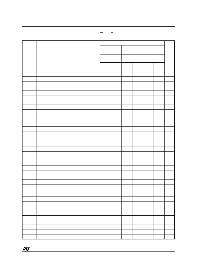
Table 10A. Read/Write Mode AC Characteristics, W and E Controlled
(T
A
= 0 to 70
°
C, –40 to 85
°
C or –40 to 125
°
C)
11/23
M28F101
相关PDF资料 |
PDF描述 |
|---|---|
| M28F101-70N3 | 1 Mb 128K x 8, Chip Erase FLASH MEMORY |
| M28F101-70N1 | 1 Mb 128K x 8, Chip Erase FLASH MEMORY |
| M28F101-120N3 | 1 Mb 128K x 8, Chip Erase FLASH MEMORY |
| M28F101-120N1 | 1 Mb 128K x 8, Chip Erase FLASH MEMORY |
| M28F101-120K6 | 1 Mb 128K x 8, Chip Erase FLASH MEMORY |
相关代理商/技术参数 |
参数描述 |
|---|---|
| M28F101-70P1 | 制造商:STMICROELECTRONICS 制造商全称:STMicroelectronics 功能描述:1 Mb 128K x 8, Chip Erase FLASH MEMORY |
| M28F101-70P3 | 制造商:STMICROELECTRONICS 制造商全称:STMicroelectronics 功能描述:1 Mb 128K x 8, Chip Erase FLASH MEMORY |
| M28F101-70P6 | 制造商:STMICROELECTRONICS 制造商全称:STMicroelectronics 功能描述:1 Mb 128K x 8, Chip Erase FLASH MEMORY |
| M28F101-70XK1 | 制造商:STMICROELECTRONICS 制造商全称:STMicroelectronics 功能描述:1 Mb 128K x 8, Chip Erase FLASH MEMORY |
| M28F101-70XK3 | 制造商:STMICROELECTRONICS 制造商全称:STMicroelectronics 功能描述:1 Mb 128K x 8, Chip Erase FLASH MEMORY |
发布紧急采购,3分钟左右您将得到回复。