- 您现在的位置:买卖IC网 > PDF目录359010 > M28F101-90N3 (意法半导体) 1 Mb 128K x 8, Chip Erase FLASH MEMORY PDF资料下载
参数资料
| 型号: | M28F101-90N3 |
| 厂商: | 意法半导体 |
| 英文描述: | 1 Mb 128K x 8, Chip Erase FLASH MEMORY |
| 中文描述: | 1 MB的128K的× 8,芯片擦除闪存 |
| 文件页数: | 17/23页 |
| 文件大小: | 197K |
| 代理商: | M28F101-90N3 |
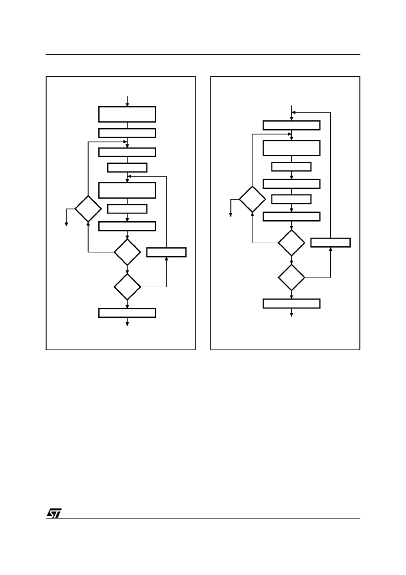
PRESTOF ERASE ALGORITHM
The PRESTO F Erase Algorithm guarantees that
the device will be erased in a reliable way. The
algorithm first programmsall bytes to 00h in order
to ensure uniform erasure. The programming fol-
lows the PRESTO F Programming Algorithm.
Erase is set-up by writing 20h to the command
register, the erasure is started by repeating this
writecycle. Erase Verifyis set-upby writing A0h to
the command registertogetherwith the addressof
the byte to be verified. The subsequentread cycle
reads the data which is compared to FFh. Erase
Verify begins at address 0000h and continues to
the last address oruntilthe comparisonof thedata
to 0FFh fails. Ifthis occurs, the addressof the last
byte checkedis stored and a newErase operation
performed. Erase Verify then continues from the
address of the stored location.
PRESTO F PROGRAMALGORITHM
The PRESTO F Programming Algorithm appliesa
series of 10
μ
s programmingpulses to a byte until
a correct verify occurs. Up to 25 programming
operations are allowed for one byte. Program is
set-upby writing 40h to the command register, the
programming is started after the next write cycle
which also latches the address and data to be
programmed. Program Verify is set-up by writing
C0h to the command register, followed by a read
cycle and a compare of the data read to the data
expected.DuringProgram and Program Verify op-
erations a MARGIN MODE circuit is activated to
guaranteethatthecellis programmedwith asafety
margin.
PROGRAM
ALL
BYTES TO 00h
AI00678
n=0, Addr=00000h
Last
Addr
ERASE SET-UP
Wait 10ms
ERASE VERIFY
Latch Addr.
READ DATA OUTPUT
Data
OK
Wait 6
μ
s
++n
LIMIT
Addr++
READ COMMAND
VPP= 12V
VPP<
6.5V
FAIL
VPP< 6.5V, PASS
YES
NO
YES
NO
YES
NO
Figure12. ErasingFlowchart
AI00677
n = 0
Last
Addr
PROGRAM VERIFY
Wait 10
μ
s
PROGRAM SET-UP
Latch Addr, Data
READ DATA OUTPUT
Data
OK
Wait 6
μ
s
++n
= 25
Addr++
READ COMMAND
VPP= 12V
VPP<
6.5V
FAIL
VPP< 6.5V, PASS
YES
NO
YES
NO
YES
NO
Figure 13. ProgrammingFlowchart
Limit:
1000 at grade 1; 6000 at grades 3 & 6.
17/23
M28F101
相关PDF资料 |
PDF描述 |
|---|---|
| M28F101-90N6 | 1 Mb 128K x 8, Chip Erase FLASH MEMORY |
| M28F101-90P3 | Quadruple 2-Line to 1-Line Data Selectors/Multiplexers With 3-State Outputs 16-SOIC 0 to 70 |
| M28F101-90P6 | 1 Mb 128K x 8, Chip Erase FLASH MEMORY |
| M28F101-90XK3 | 1 Mb 128K x 8, Chip Erase FLASH MEMORY |
| M28F101-90XK6 | 1 Mb 128K x 8, Chip Erase FLASH MEMORY |
相关代理商/技术参数 |
参数描述 |
|---|---|
| M28F101-90N6 | 制造商:STMICROELECTRONICS 制造商全称:STMicroelectronics 功能描述:1 Mb 128K x 8, Chip Erase FLASH MEMORY |
| M28F101-90P1 | 制造商:STMICROELECTRONICS 制造商全称:STMicroelectronics 功能描述:1 Mb 128K x 8, Chip Erase FLASH MEMORY |
| M28F101-90P3 | 制造商:STMICROELECTRONICS 制造商全称:STMicroelectronics 功能描述:1 Mb 128K x 8, Chip Erase FLASH MEMORY |
| M28F101-90P6 | 制造商:STMICROELECTRONICS 制造商全称:STMicroelectronics 功能描述:1 Mb 128K x 8, Chip Erase FLASH MEMORY |
| M28F101-90XK1 | 制造商:STMICROELECTRONICS 制造商全称:STMicroelectronics 功能描述:1 Mb 128K x 8, Chip Erase FLASH MEMORY |
发布紧急采购,3分钟左右您将得到回复。