- 您现在的位置:买卖IC网 > PDF目录359014 > M28LV64-250XMS1 (意法半导体) 64K 8K x 8 LOW VOLTAGE PARALLEL EEPROM with SOFTWARE DATA PROTECTION PDF资料下载
参数资料
| 型号: | M28LV64-250XMS1 |
| 厂商: | 意法半导体 |
| 元件分类: | EEPROM |
| 英文描述: | 64K 8K x 8 LOW VOLTAGE PARALLEL EEPROM with SOFTWARE DATA PROTECTION |
| 中文描述: | 64K的8K的× 8低电压并联EEPROM,带有软件数据保护 |
| 文件页数: | 4/18页 |
| 文件大小: | 127K |
| 代理商: | M28LV64-250XMS1 |
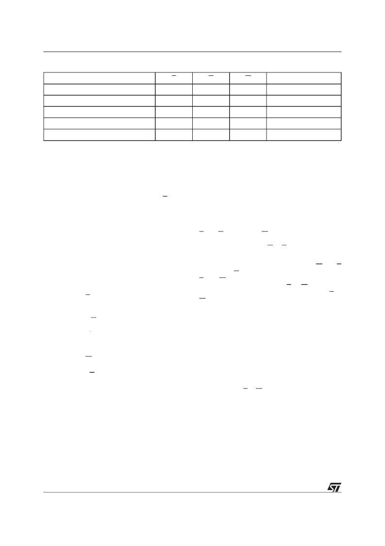
Mode
E
G
W
DQ0 - DQ7
Standby
1
X
X
Hi-Z
Output Disable
X
1
X
Hi-Z
Write Disable
X
X
1
Hi-Z
Read
0
0
1
Data Out
Write
0
1
0
Data In
Note:
1. 0 = V
IL
; 1 = V
IH
; X =V
IL
or V
IH
.
Table 3. OperatingModes
(1)
The M28LV64 outputs the Ready/Busy write
status,theM28LV64-aaaX(aaa=accesstime)has
no Ready/Busystatus and the relevant RB pin is
Not Connected (NC). The circuit has been de-
signed to offer a flexible microcontroller interface
featuring both hardware and software handshak-
ing with Ready/Busy,Data Polling and ToggleBit.
The M28LV64 supports 64 byte page write opera-
tion. A Software Data Protection (SDP) is also
possibleusing the standard JEDEC algorithm.
PINDESCRIPTION
Addresses (A0-A12).
The address inputs select
an 8-bit memory location during a read or write
operation.
Chip Enable (E).
The chip enable input must be
low to enableall read/writeoperations.WhenChip
Enableis high, power consumptionis reduced.
Output Enable (G).
TheOutput Enableinput con-
trols the data outputbuffersand is used to initiate
read operations.
DataIn/Out(DQ0- DQ7).
Datais written toorread
from the M28LV64 through the I/O pins.
Write Enable (W).
The Write Enableinputcontrols
the writing of data to the M28LV64.
Ready/Busy (RB).
Ready/Busy is an open drain
output that can be used to detect the end of the
internalwritecycle (thisfunctionappliesonlyto the
M28LV64).
OPERATION
In order to preventdata corruption andinadvertent
writeoperationsaninternalV
CC
comparatorinhibits
Write operation if V
CC
is below V
WI
(see Table 6).
Accesstothememory inwritemodeisallowedafter
a power-up as specifiedin Table6.
Read
TheM28LV64isaccessedlikea staticRAM. When
E and G are low with W high, the data addressed
is presented on the I/O pins. The I/O pinsare high
impedancewhen either G or E is high.
Write
Write operationsare initiated when both W and E
are low and G is high.TheM28LV64 supports both
E and W controlled write cycles. The Address is
latched by the falling edge of E or W which ever
occurslast and the Data on the rising edge of E or
W which ever occurs first. Once initiated the write
operationis internallytimed untilcompletion.
Page Write
Page write allows up to 64 bytes to be consecu-
tively latched into the memory prior to initiating a
programming cycle. All bytes must be located in a
single page address, that is A6-A12 must be the
samefor all bytes. The page writecan beinitiated
duringany byte write operation.
Following the first byte write instruction the host
may send another address and data with a mini-
mum data transfer rate of t
WHWH
(see Figure 13).
If atransitionof Eor Wisnotdetectedwithin t
WHWH
the internal programming cyclewill start.
DESCRIPTION
(cont’d)
4/18
M28LV64
相关PDF资料 |
PDF描述 |
|---|---|
| M28LV64-200XMS1 | 64K 8K x 8 LOW VOLTAGE PARALLEL EEPROM with SOFTWARE DATA PROTECTION |
| M28W160ECB | 16 Mbit (1Mb x16, Boot Block) 3V Supply Flash Memory |
| M28W160ECB100N1E | 16 Mbit (1Mb x16, Boot Block) 3V Supply Flash Memory |
| M28W160ECB100N1F | 16 Mbit (1Mb x16, Boot Block) 3V Supply Flash Memory |
| M28W160ECB100N1S | 16 Mbit (1Mb x16, Boot Block) 3V Supply Flash Memory |
相关代理商/技术参数 |
参数描述 |
|---|---|
| M28LV64-250XMS6 | 制造商:STMICROELECTRONICS 制造商全称:STMicroelectronics 功能描述:64K 8K x 8 LOW VOLTAGE PARALLEL EEPROM with SOFTWARE DATA PROTECTION |
| M28LV64-250XN1 | 制造商:STMICROELECTRONICS 制造商全称:STMicroelectronics 功能描述:64K 8K x 8 LOW VOLTAGE PARALLEL EEPROM with SOFTWARE DATA PROTECTION |
| M28LV64-250XN6 | 制造商:STMICROELECTRONICS 制造商全称:STMicroelectronics 功能描述:64K 8K x 8 LOW VOLTAGE PARALLEL EEPROM with SOFTWARE DATA PROTECTION |
| M28LV64-250XP1 | 制造商:STMICROELECTRONICS 制造商全称:STMicroelectronics 功能描述:64K 8K x 8 LOW VOLTAGE PARALLEL EEPROM with SOFTWARE DATA PROTECTION |
| M28LV64-250XP6 | 制造商:STMICROELECTRONICS 制造商全称:STMicroelectronics 功能描述:64K 8K x 8 LOW VOLTAGE PARALLEL EEPROM with SOFTWARE DATA PROTECTION |
发布紧急采购,3分钟左右您将得到回复。