- 您现在的位置:买卖IC网 > PDF目录359024 > M29F016B90N3T (意法半导体) 16 Mbit 2Mb x8, Uniform Block Single Supply Flash Memory PDF资料下载
参数资料
| 型号: | M29F016B90N3T |
| 厂商: | 意法半导体 |
| 英文描述: | 16 Mbit 2Mb x8, Uniform Block Single Supply Flash Memory |
| 中文描述: | 16兆位的2Mb × 8,统一座单电源闪存 |
| 文件页数: | 4/22页 |
| 文件大小: | 135K |
| 代理商: | M29F016B90N3T |
M29F016B
4/22
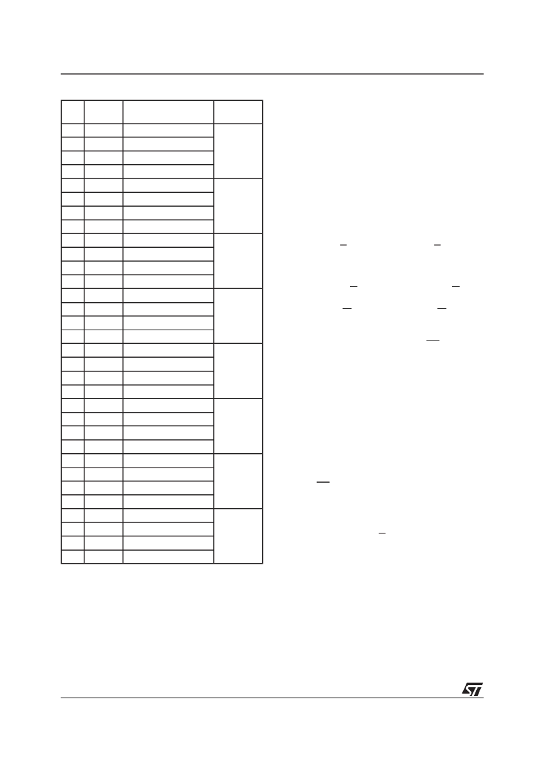
Table 3. Uniform Block Addresses, M29F016B
Size
(Kbytes)
#
Address Range
Protection
Group
31
64
1F0000h-1FFFFFh
7
30
64
1E0000h-1EFFFFh
29
64
1D0000h-1DFFFFh
28
64
1C0000h-1CFFFFh
27
64
1B0000h-1BFFFFh
6
26
64
1A0000h-1AFFFFh
25
64
190000h-19FFFFh
24
64
180000h-18FFFFh
23
64
170000h-17FFFFh
5
22
64
160000h-16FFFFh
21
64
150000h-15FFFFh
20
64
140000h-14FFFFh
19
64
130000h-13FFFFh
4
18
64
120000h-12FFFFh
17
64
110000h-11FFFFh
16
64
100000h-10FFFFh
15
64
0F0000h-0FFFFFh
3
14
64
0E0000h-0EFFFFh
13
64
0D0000h-0DFFFFh
12
64
0C0000h-0CFFFFh
11
64
0B0000h-0BFFFFh
2
10
64
0A0000h-0AFFFFh
9
64
090000h-09FFFFh
8
64
080000h-08FFFFh
7
64
070000h-07FFFFh
1
6
64
060000h-06FFFFh
5
64
050000h-05FFFFh
4
64
040000h-04FFFFh
3
64
030000h-03FFFFh
0
2
64
020000h-02FFFFh
1
64
010000h-01FFFFh
0
64
000000h-00FFFFh
SIGNAL DESCRIPTIONS
See Figure 1, Logic Diagram, and Table 1, Signal
Names, for a brief overview of the signals connect-
ed to this device.
Address Inputs (A0-A20).
The Address Inputs
select the cells in the memory array to access dur-
ing Bus Read operations. During Bus Write opera-
tions they control the commands sent to the
Command Interface of the internal state machine.
Data Inputs/Outputs (DQ0-DQ7).
The Data In-
puts/Outputs output thedata stored atthe selected
address during a Bus Read operation. During Bus
Write operations they represent the commands
sentto the Command Interfaceof theinternal state
machine.
Chip Enable (E).
The Chip Enable, E, activates
the memory, allowing Bus Read and Bus Write op-
erations to be performed. When Chip Enable is
High, V
IH
, all other pins are ignored.
Output Enable (G).
The Output Enable, G, con-
trols the Bus Read operation of the memory.
Write Enable (W).
The Write Enable, W, controls
the Bus Write operation of the memory’s Com-
mand Interface.
Reset/Block Temporary Unprotect (RP).
The Re-
set/Block Temporary Unprotect pin can be usedto
apply a Hardware Reset to the memory or to tem-
porarily unprotect all blocks that have been pro-
tected.
A Hardware Reset is achieved by holding Reset/
Block Temporary Unprotect Low, V
IL
, for at least
t
PLPX
. After Reset/Block Temporary Unprotect
goes High, V
IH
, the memory will be ready for Bus
Read and Bus Write operations after t
PHEL
or
t
RHEL
, whicheveroccurs last.See theReady/Busy
Output section, Table 14 and Figure 11, Reset/
Temporary Unprotect AC Characteristics for more
details.
Holding RP at V
ID
will temporarily unprotect the
protected blocks in the memory. Program and
Erase operations on all blocks will be possible.
The transition from V
IH
toV
ID
must be slower than
t
PHPHH
.
Ready/Busy Output (RB).
The Ready/Busy pin
is an open-drain outputthat canbe used to identify
when the memory array can be read. Ready/Busy
is high-impedance during Read mode,Auto Select
mode and Erase Suspend mode.
相关PDF资料 |
PDF描述 |
|---|---|
| M29F016B90N6T | 16 Mbit 2Mb x8, Uniform Block Single Supply Flash Memory |
| M29F016B70M1T | 16 Mbit 2Mb x8, Uniform Block Single Supply Flash Memory |
| M29F016B70M3T | 16 Mbit 2Mb x8, Uniform Block Single Supply Flash Memory |
| M29F016B70M6T | 16 Mbit 2Mb x8, Uniform Block Single Supply Flash Memory |
| M29F016B70N1T | 16 Mbit 2Mb x8, Uniform Block Single Supply Flash Memory |
相关代理商/技术参数 |
参数描述 |
|---|---|
| M29F016B90N6T | 制造商:STMICROELECTRONICS 制造商全称:STMicroelectronics 功能描述:16 Mbit 2Mb x8, Uniform Block Single Supply Flash Memory |
| M29F016D | 制造商:AMD 制造商全称:Advanced Micro Devices 功能描述:16 Megabit (2 M x 8-Bit) CMOS 5.0 Volt-only, Uniform Sector Flash Memory |
| M29F016D_05 | 制造商:STMICROELECTRONICS 制造商全称:STMicroelectronics 功能描述:16 Mbit (2Mb x8, Uniform Block) 5V Supply Flash Memory |
| M29F016D55M1T | 制造商:STMICROELECTRONICS 制造商全称:STMicroelectronics 功能描述:16 Mbit (2Mb x8, Uniform Block) 5V Supply Flash Memory |
| M29F016D55M6T | 制造商:STMICROELECTRONICS 制造商全称:STMicroelectronics 功能描述:16 Mbit (2Mb x8, Uniform Block) 5V Supply Flash Memory |
发布紧急采购,3分钟左右您将得到回复。