- 您现在的位置:买卖IC网 > PDF目录359053 > M29W800AB80ZA5T (意法半导体) 8 Mbit 1Mb x8 or 512Kb x16, Boot Block Low Voltage Single Supply Flash Memory PDF资料下载
参数资料
| 型号: | M29W800AB80ZA5T |
| 厂商: | 意法半导体 |
| 英文描述: | 8 Mbit 1Mb x8 or 512Kb x16, Boot Block Low Voltage Single Supply Flash Memory |
| 中文描述: | 8兆1兆x8或512KB的x16插槽,引导块低压单电源闪存 |
| 文件页数: | 18/33页 |
| 文件大小: | 234K |
| 代理商: | M29W800AB80ZA5T |
第1页第2页第3页第4页第5页第6页第7页第8页第9页第10页第11页第12页第13页第14页第15页第16页第17页当前第18页第19页第20页第21页第22页第23页第24页第25页第26页第27页第28页第29页第30页第31页第32页第33页
M29W800AT, M29W800AB
18/33
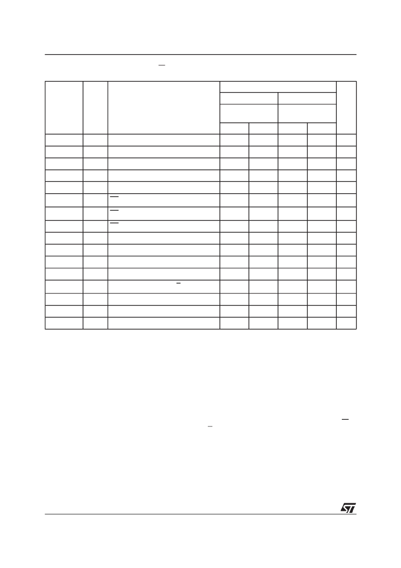
Table 18. Write AC Characteristics, W Controlled
(T
A
= 0 to 70
°
C, –20 to 85
°
C or –40 to 85
°
C)
Note: 1. Sampled only, not 100% tested.
2. This timing is for Temporary Block Unprotection operation.
Symbol
Alt
Parameter
M29W800AT / M29W800AB
Unit
100
120
V
CC
= 2.7V to 3.6V
CL = 30pF
V
CC
= 2.7V to 3.6V
CL = 30pF
Min
Max
Min
Max
t
AVAV
t
WC
Address Valid to Next Address Valid
100
120
ns
t
AVWL
t
AS
Address Valid to Write Enable Low
0
0
ns
t
DVWH
t
DS
Input Valid to Write Enable High
45
50
ns
t
ELWL
t
CS
Chip Enable Low to Write Enable Low
0
0
ns
t
GHWL
Output Enable High to Write Enable Low
0
0
ns
t
PHPHH(1, 2)
t
VIDR
RP Rise Time to V
ID
500
500
ns
t
PHWL(1)
t
RSP
RP High to Write Enable Low
4
4
μ
s
t
PLPX
t
RP
RP Pulse Width
500
500
ns
t
VCHEL
t
VCS
V
CC
High to Chip Enable Low
50
50
μ
s
t
WHDX
t
DH
Write Enable High to Input Transition
0
0
ns
t
WHEH
t
CH
Write Enable High to Chip Enable High
0
0
ns
t
WHGL
t
OEH
Write Enable High to Output Enable Low
0
0
ns
t
WHRL(1)
t
BUSY
Program Erase Valid to RB Delay
90
90
ns
t
WHWL
t
WPH
Write Enable High to Write Enable Low
30
30
ns
t
WLAX
t
AH
Write Enable Low to Address Transition
45
50
ns
t
WLWH
t
WP
Write Enable Low to Write Enable High
35
50
ns
During the execution of the erase by the P/E.C.,
the memory accepts only the Erase Suspend ES
and Read/Reset RD instructions. Data Polling bit
DQ7 returns ’0’ while the erasure is in progress
and ’1’ when it has completed. The Toggle bit DQ2
and DQ6 toggle during the erase operation. They
stop when erase is completed. After completion
the Status Register bit DQ5 returns ’1’if there has
been an erasefailure. In such a situation, theTog-
gle bit DQ2 can be used to determine which block
is notcorrectly erased. In the caseof erase failure,
a Read/ResetRD instruction is necessary inorder
to reset the P/E.C.
Chip Erase (CE) Instruction.
This
uses six write cycles. The Erase Set-up command
80h is written to address AAAh in the Byte-wide
configuration or the address 555h in the Word-
instruction
wide configuration on the third cycle after the two
Coded cycles. The Chip Erase Confirm command
10h is similarly written on the sixth cycle after an-
other two Coded cycles. If the second command
given is not an erase confirm or if the Coded cy-
cles are wrong, the instruction aborts and the de-
vice is reset to Read Array. It is not necessary to
program the array with 00h first as the P/E.C. will
automatically do this before erasing it to FFh.
Read operations afterthe sixth rising edge of W or
E output the Status Register bits. During the exe-
cution of the erase by the P/E.C., Data Polling bit
DQ7 returns ’0’,then ’1’oncompletion. TheToggle
bits DQ2 and DQ6 toggle during erase operation
and stop when erase is completed. After comple-
tion the Status Register bit DQ5 returns ’1’if there
has been an Erase Failure.
相关PDF资料 |
PDF描述 |
|---|---|
| M29W800AT80ZA5T | 8 Mbit 1Mb x8 or 512Kb x16, Boot Block Low Voltage Single Supply Flash Memory |
| M29W800AB90M6T | Circular Connector; No. of Contacts:12; Series:JT02R; Body Material:Aluminum; Connecting Termination:Crimp; Connector Shell Size:14; Circular Contact Gender:Pin; Circular Shell Style:Box Mount Receptacle; Insert Arrangement:14-97 |
| M29W800AB90M5T | Circular Connector; No. of Contacts:37; Series:JT02R; Body Material:Aluminum; Connecting Termination:Crimp; Connector Shell Size:14; Circular Contact Gender:Socket; Circular Shell Style:Box Mount Receptacle; Insert Arrangement:14-37 |
| M29W800AB90M1T | Circular Connector; No. of Contacts:37; Series:JT02R; Body Material:Aluminum; Connecting Termination:Crimp; Connector Shell Size:14; Circular Contact Gender:Pin; Circular Shell Style:Box Mount Receptacle; Insert Arrangement:14-37 |
| M29W800AB90N1T | Circular Connector; No. of Contacts:55; Series:JT02R; Body Material:Aluminum; Connecting Termination:Crimp; Connector Shell Size:16; Circular Contact Gender:Socket; Circular Shell Style:Box Mount Receptacle; Insert Arrangement:16-55 |
相关代理商/技术参数 |
参数描述 |
|---|---|
| M29W800AB90M1 | 功能描述:闪存 RO 511-M29W800DB70N RoHS:否 制造商:ON Semiconductor 数据总线宽度:1 bit 存储类型:Flash 存储容量:2 MB 结构:256 K x 8 定时类型: 接口类型:SPI 访问时间: 电源电压-最大:3.6 V 电源电压-最小:2.3 V 最大工作电流:15 mA 工作温度:- 40 C to + 85 C 安装风格:SMD/SMT 封装 / 箱体: 封装:Reel |
| M29W800AB90N1 | 功能描述:电可擦除可编程只读存储器 1Mx8 or 512Kx16 90ns RoHS:否 制造商:Atmel 存储容量:2 Kbit 组织:256 B x 8 数据保留:100 yr 最大时钟频率:1000 KHz 最大工作电流:6 uA 工作电源电压:1.7 V to 5.5 V 最大工作温度:+ 85 C 安装风格:SMD/SMT 封装 / 箱体:SOIC-8 |
| M29W800AB90N1T | 制造商:Micron Technology Inc 功能描述:FLASH PARALLEL 3.3V 8MBIT 1MX8/512KX16 90NS 48TSOP - Tape and Reel |
| M29W800AB90N6 | 功能描述:闪存 1Mx8 or 512Kx16 90ns RoHS:否 制造商:ON Semiconductor 数据总线宽度:1 bit 存储类型:Flash 存储容量:2 MB 结构:256 K x 8 定时类型: 接口类型:SPI 访问时间: 电源电压-最大:3.6 V 电源电压-最小:2.3 V 最大工作电流:15 mA 工作温度:- 40 C to + 85 C 安装风格:SMD/SMT 封装 / 箱体: 封装:Reel |
| M29W800AT100N1 | 功能描述:闪存 1Mx8 or 512Kx16 100n RoHS:否 制造商:ON Semiconductor 数据总线宽度:1 bit 存储类型:Flash 存储容量:2 MB 结构:256 K x 8 定时类型: 接口类型:SPI 访问时间: 电源电压-最大:3.6 V 电源电压-最小:2.3 V 最大工作电流:15 mA 工作温度:- 40 C to + 85 C 安装风格:SMD/SMT 封装 / 箱体: 封装:Reel |
发布紧急采购,3分钟左右您将得到回复。