- 您现在的位置:买卖IC网 > PDF目录377821 > M29W800DB45N6T (意法半导体) 8 Mbit (1Mb x8 or 512Kb x16, Boot Block) 3V Supply Flash Memory PDF资料下载
参数资料
| 型号: | M29W800DB45N6T |
| 厂商: | 意法半导体 |
| 英文描述: | 8 Mbit (1Mb x8 or 512Kb x16, Boot Block) 3V Supply Flash Memory |
| 中文描述: | 8兆(1兆x8或512KB的x16插槽,引导块)3V电源快闪记忆体 |
| 文件页数: | 36/42页 |
| 文件大小: | 275K |
| 代理商: | M29W800DB45N6T |
第1页第2页第3页第4页第5页第6页第7页第8页第9页第10页第11页第12页第13页第14页第15页第16页第17页第18页第19页第20页第21页第22页第23页第24页第25页第26页第27页第28页第29页第30页第31页第32页第33页第34页第35页当前第36页第37页第38页第39页第40页第41页第42页
M29W800DT, M29W800DB
36/42
APPENDIX C. BLOCK PROTECTION
Block protection can be used to prevent any oper-
ation from modifying the data stored in the Flash.
Each Block can be protected individually. Once
protected, Program and Erase operations on the
block fail to change the data.
There are three techniques that can be used to
control Block Protection, these are the Program-
mer technique, the In-System technique and Tem-
porary Unprotection. Temporary Unprotection is
controlled by the Reset/Block Temporary Unpro-
tection pin, RP; this is described in the Signal De-
scriptions section.
Unlike the Command Interface of the Program/
Erase Controller, the techniques for protecting and
unprotecting blocks change between different
Flash memory suppliers. For example, the tech-
niques for AMD parts will not work on STMicro-
electronics parts. Care should be taken when
changing drivers for one part to work on another.
Programmer Technique
The Programmer technique uses high (V
ID
) volt-
age levels on some of the bus pins. These cannot
be achieved using a standard microprocessor bus,
therefore the technique is recommended only for
use in Programming Equipment.
To protect a block follow the flowchart in
Figure
20., Programmer Equipment Block Protect Flow-
chart
, To unprotect the whole chip it is necessary
to protect all of the blocks first, then all blocks can
be unprotected at the same time. To unprotect the
chip follow
Figure 21., Programmer Equipment
Chip Unprotect Flowchart
.
Table 29., Programmer
Technique Bus Operations, BYTE = V
IH
or V
IL
,
gives a summary of each operation.
The timing on these flowcharts is critical. Care
should be taken to ensure that, where a pause is
specified, it is followed as closely as possible. Do
not abort the procedure before reaching the end.
Chip Unprotect can take several seconds and a
user message should be provided to show that the
operation is progressing.
In-System Technique
The In-System technique requires a high voltage
level on the Reset/Blocks Temporary Unprotect
pin, RP. This can be achieved without violating the
maximum ratings of the components on the micro-
processor bus, therefore this technique is suitable
for use after the Flash has been fitted to the sys-
tem.
To protect a block follow the flowchart in
Figure
22., In-System Equipment Block Protect Flow-
chart
. To unprotect the whole chip it is necessary
to protect all of the blocks first, then all the blocks
can be unprotected at the same time. To unprotect
the chip follow
Figure 23., In-System Equipment
Chip Unprotect Flowchart
.
The timing on these flowcharts is critical. Care
should be taken to ensure that, where a pause is
specified, it is followed as closely as possible. Do
not allow the microprocessor to service interrupts
that will upset the timing and do not abort the pro-
cedure before reaching the end. Chip Unprotect
can take several seconds and a user message
should be provided to show that the operation is
progressing.
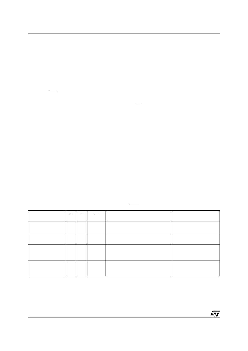
Table 29. Programmer Technique Bus Operations, BYTE = V
IH
or V
IL
Operation
E
G
W
Address Inputs
A0-A18
Data Inputs/Outputs
DQ15A–1, DQ14-DQ0
Block Protect
V
IL
V
ID
V
IL
Pulse
A9 = V
ID
, A12-A18 Block Address
Others = X
X
Chip Unprotect
V
ID
V
ID
V
IL
Pulse
A9 = V
ID
, A12 = V
IH
, A15 = V
IH
Others = X
X
Block Protection
Verify
V
IL
V
IL
V
IH
A0 = V
IL
, A1 = V
IH
, A6 = V
IL
, A9 = V
ID
,
A12-A18 Block Address
Others = X
Pass = XX01h
Retry = XX00h
Block Unprotection
Verify
V
IL
V
IL
V
IH
A0 = V
IL
, A1 = V
IH
, A6 = V
IH
, A9 = V
ID
,
A12-A18 Block Address
Others = X
Retry = XX01h
Pass = XX00h
相关PDF资料 |
PDF描述 |
|---|---|
| M29W800DB45ZA1E | 8 Mbit (1Mb x8 or 512Kb x16, Boot Block) 3V Supply Flash Memory |
| M29W800DB45ZA1F | 8 Mbit (1Mb x8 or 512Kb x16, Boot Block) 3V Supply Flash Memory |
| M29W800DB45ZA1T | 8 Mbit (1Mb x8 or 512Kb x16, Boot Block) 3V Supply Flash Memory |
| M29W800DB45ZA6E | 8 Mbit (1Mb x8 or 512Kb x16, Boot Block) 3V Supply Flash Memory |
| M29W800DB45ZA6F | 8 Mbit (1Mb x8 or 512Kb x16, Boot Block) 3V Supply Flash Memory |
相关代理商/技术参数 |
参数描述 |
|---|---|
| M29W800DB45ZE6E | 功能描述:闪存 8 MBIT (1MB) 3V SUPPLY RoHS:否 制造商:ON Semiconductor 数据总线宽度:1 bit 存储类型:Flash 存储容量:2 MB 结构:256 K x 8 定时类型: 接口类型:SPI 访问时间: 电源电压-最大:3.6 V 电源电压-最小:2.3 V 最大工作电流:15 mA 工作温度:- 40 C to + 85 C 安装风格:SMD/SMT 封装 / 箱体: 封装:Reel |
| M29W800DB45ZE6F | 功能描述:闪存 STD FLASH RoHS:否 制造商:ON Semiconductor 数据总线宽度:1 bit 存储类型:Flash 存储容量:2 MB 结构:256 K x 8 定时类型: 接口类型:SPI 访问时间: 电源电压-最大:3.6 V 电源电压-最小:2.3 V 最大工作电流:15 mA 工作温度:- 40 C to + 85 C 安装风格:SMD/SMT 封装 / 箱体: 封装:Reel |
| M29W800DB45ZE6F TR | 制造商:Micron Technology Inc 功能描述:IC FLASH 8MBIT 45NS 48TFBGA |
| M29W800DB70M6 | 功能描述:闪存 1Mx8 or 512Kx16 70ns RoHS:否 制造商:ON Semiconductor 数据总线宽度:1 bit 存储类型:Flash 存储容量:2 MB 结构:256 K x 8 定时类型: 接口类型:SPI 访问时间: 电源电压-最大:3.6 V 电源电压-最小:2.3 V 最大工作电流:15 mA 工作温度:- 40 C to + 85 C 安装风格:SMD/SMT 封装 / 箱体: 封装:Reel |
| M29W800DB70N1 | 功能描述:闪存 1Mx8 or 512Kx16 70ns RoHS:否 制造商:ON Semiconductor 数据总线宽度:1 bit 存储类型:Flash 存储容量:2 MB 结构:256 K x 8 定时类型: 接口类型:SPI 访问时间: 电源电压-最大:3.6 V 电源电压-最小:2.3 V 最大工作电流:15 mA 工作温度:- 40 C to + 85 C 安装风格:SMD/SMT 封装 / 箱体: 封装:Reel |
发布紧急采购,3分钟左右您将得到回复。