- 您现在的位置:买卖IC网 > PDF目录359053 > M29W800DB70M6T (意法半导体) Low-Power Configurable Multiple-Function Gate 6-SOT-23 -40 to 85 PDF资料下载
参数资料
| 型号: | M29W800DB70M6T |
| 厂商: | 意法半导体 |
| 英文描述: | Low-Power Configurable Multiple-Function Gate 6-SOT-23 -40 to 85 |
| 中文描述: | 8兆(1兆x8或512KB的x16插槽,引导块)3V电源快闪记忆体 |
| 文件页数: | 32/41页 |
| 文件大小: | 219K |
| 代理商: | M29W800DB70M6T |
第1页第2页第3页第4页第5页第6页第7页第8页第9页第10页第11页第12页第13页第14页第15页第16页第17页第18页第19页第20页第21页第22页第23页第24页第25页第26页第27页第28页第29页第30页第31页当前第32页第33页第34页第35页第36页第37页第38页第39页第40页第41页
M29W800DT, M29W800DB
32/41
APPENDIX B. COMMON FLASH INTERFACE (CFI)
The Common Flash Interface is a JEDEC ap-
proved, standardized data structure that can be
read from the Flash memory device. It allows a
system software to query the device to determine
various electrical and timing parameters, density
information and functions supported by the mem-
ory. The system can interface easily with the de-
vice, enabling the software to upgrade itself when
necessary.
When the CFI Query Command is issued the de-
vice enters CFI Query mode and the data structure
is read from the memory. Tables 20, 21, 22, 23, 24
and 24 show the addresses used to retrieve the
data.
The CFI data structure also contains a security
area where a 64 bit unique security number is writ-
ten (see Table , Security Code area). This area
can be accessed only in Read mode by the final
user. It is impossible to change the security num-
ber after it has been written by ST. Issue a Read
command to return to Read mode.
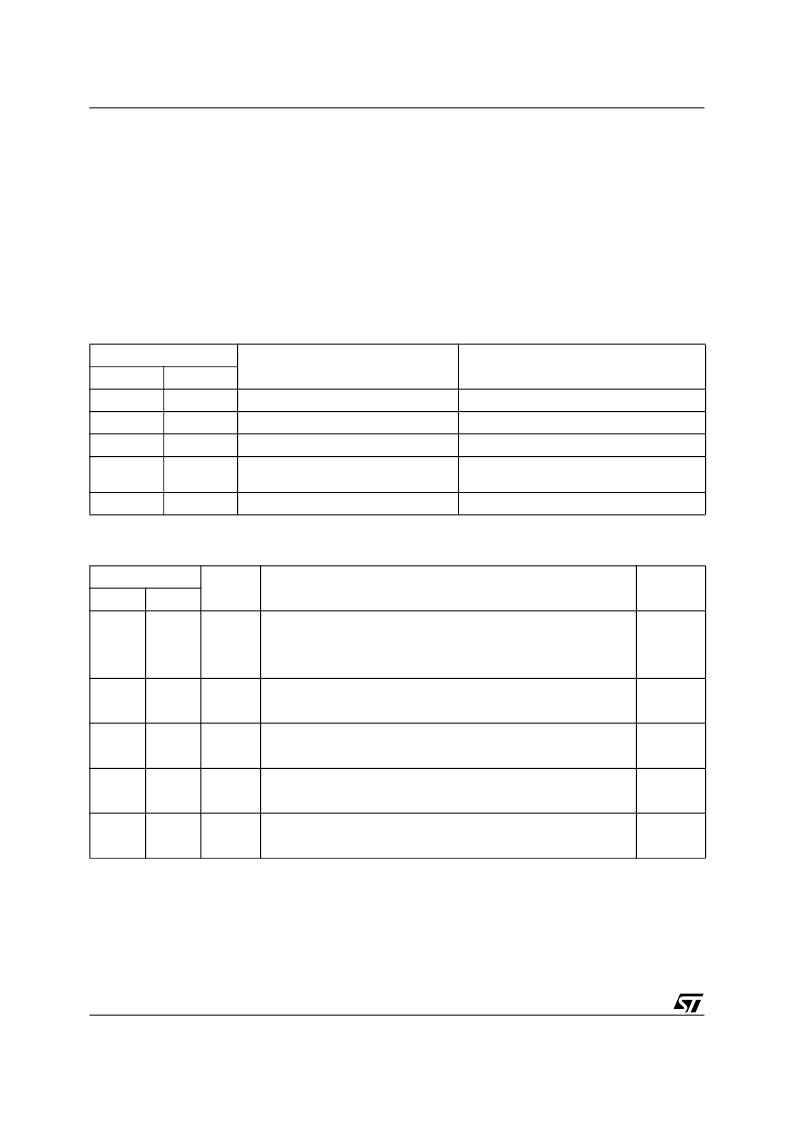
Table 20. Query Structure Overview
Note: Query data are always presented on the lowest order data outputs.
Table 21. CFI Query Identification String
Note:
Query data are always presented on the lowest order data outputs (DQ7-DQ0) only. DQ8-DQ15 are ‘0’.
Address
Sub-section Name
Description
x16
x8
10h
20h
CFI Query Identification String
Command set ID and algorithm data offset
1Bh
36h
System Interface Information
Device timing & voltage information
27h
4Eh
Device Geometry Definition
Flash device layout
40h
80h
Primary Algorithm-specific Extended
Query table
Additional information specific to the Primary
Algorithm (optional)
61h
C2h
Security Code Area
64 bit unique device number
Address
Data
Description
Value
x16
x8
10h
20h
0051h
"Q"
11h
22h
0052h
Query Unique ASCII String "QRY"
"R"
12h
24h
0059h
"Y"
13h
26h
0002h
Primary Algorithm Command Set and Control Interface ID code 16 bit
ID code defining a specific algorithm
AMD
Compatible
14h
28h
0000h
15h
2Ah
0040h
Address for Primary Algorithm extended Query table (see Table 23)
P = 40h
16h
2Ch
0000h
17h
2Eh
0000h
Alternate Vendor Command Set and Control Interface ID Code second
vendor - specified algorithm supported
NA
18h
30h
0000h
19h
32h
0000h
Address for Alternate Algorithm extended Query table
NA
1Ah
34h
0000h
相关PDF资料 |
PDF描述 |
|---|---|
| M29W800DB70N1T | Low-Power Configurable Multiple-Function Gate 6-SC70 -40 to 85 |
| M29W800DB70N6T | Low-Power Configurable Multiple-Function Gate 6-SC70 -40 to 85 |
| M29W800DB70ZA1T | Low-Power Configurable Multiple-Function Gate 6-SC70 -40 to 85 |
| M29W800DB70ZA6T | Low-Power Configurable Multiple-Function Gate 6-SC70 -40 to 85 |
| M29W800DB90N1T | Low-Power Configurable Multiple-Function Gate 6-SC70 -40 to 85 |
相关代理商/技术参数 |
参数描述 |
|---|---|
| M29W800DB70N1 | 功能描述:闪存 1Mx8 or 512Kx16 70ns RoHS:否 制造商:ON Semiconductor 数据总线宽度:1 bit 存储类型:Flash 存储容量:2 MB 结构:256 K x 8 定时类型: 接口类型:SPI 访问时间: 电源电压-最大:3.6 V 电源电压-最小:2.3 V 最大工作电流:15 mA 工作温度:- 40 C to + 85 C 安装风格:SMD/SMT 封装 / 箱体: 封装:Reel |
| M29W800DB70N3T | 功能描述:闪存 1Mx8 or 512Kx16 70ns RoHS:否 制造商:ON Semiconductor 数据总线宽度:1 bit 存储类型:Flash 存储容量:2 MB 结构:256 K x 8 定时类型: 接口类型:SPI 访问时间: 电源电压-最大:3.6 V 电源电压-最小:2.3 V 最大工作电流:15 mA 工作温度:- 40 C to + 85 C 安装风格:SMD/SMT 封装 / 箱体: 封装:Reel |
| M29W800DB70N6 | 功能描述:闪存 1Mx8 or 512Kx16 70ns RoHS:否 制造商:ON Semiconductor 数据总线宽度:1 bit 存储类型:Flash 存储容量:2 MB 结构:256 K x 8 定时类型: 接口类型:SPI 访问时间: 电源电压-最大:3.6 V 电源电压-最小:2.3 V 最大工作电流:15 mA 工作温度:- 40 C to + 85 C 安装风格:SMD/SMT 封装 / 箱体: 封装:Reel |
| M29W800DB-70N6 | 制造商:STMicroelectronics 功能描述:NOR Flash, 512K x 16, 48 Pin, Plastic, TSSOP |
| M29W800DB70N6E | 功能描述:闪存 1Mx8 or 512Kx16 70ns RoHS:否 制造商:ON Semiconductor 数据总线宽度:1 bit 存储类型:Flash 存储容量:2 MB 结构:256 K x 8 定时类型: 接口类型:SPI 访问时间: 电源电压-最大:3.6 V 电源电压-最小:2.3 V 最大工作电流:15 mA 工作温度:- 40 C to + 85 C 安装风格:SMD/SMT 封装 / 箱体: 封装:Reel |
发布紧急采购,3分钟左右您将得到回复。