- 您现在的位置:买卖IC网 > PDF目录45011 > M30260F3AGP-U3 16-BIT, FLASH, 20 MHz, MICROCONTROLLER, PQFP48 PDF资料下载
参数资料
| 型号: | M30260F3AGP-U3 |
| 元件分类: | 微控制器/微处理器 |
| 英文描述: | 16-BIT, FLASH, 20 MHz, MICROCONTROLLER, PQFP48 |
| 封装: | 7 X 7 MM, 0.50 MM PITCH, LEAD FREE, PLASTIC, LQFP-48 |
| 文件页数: | 33/352页 |
| 文件大小: | 2423K |
| 代理商: | M30260F3AGP-U3 |
第1页第2页第3页第4页第5页第6页第7页第8页第9页第10页第11页第12页第13页第14页第15页第16页第17页第18页第19页第20页第21页第22页第23页第24页第25页第26页第27页第28页第29页第30页第31页第32页当前第33页第34页第35页第36页第37页第38页第39页第40页第41页第42页第43页第44页第45页第46页第47页第48页第49页第50页第51页第52页第53页第54页第55页第56页第57页第58页第59页第60页第61页第62页第63页第64页第65页第66页第67页第68页第69页第70页第71页第72页第73页第74页第75页第76页第77页第78页第79页第80页第81页第82页第83页第84页第85页第86页第87页第88页第89页第90页第91页第92页第93页第94页第95页第96页第97页第98页第99页第100页第101页第102页第103页第104页第105页第106页第107页第108页第109页第110页第111页第112页第113页第114页第115页第116页第117页第118页第119页第120页第121页第122页第123页第124页第125页第126页第127页第128页第129页第130页第131页第132页第133页第134页第135页第136页第137页第138页第139页第140页第141页第142页第143页第144页第145页第146页第147页第148页第149页第150页第151页第152页第153页第154页第155页第156页第157页第158页第159页第160页第161页第162页第163页第164页第165页第166页第167页第168页第169页第170页第171页第172页第173页第174页第175页第176页第177页第178页第179页第180页第181页第182页第183页第184页第185页第186页第187页第188页第189页第190页第191页第192页第193页第194页第195页第196页第197页第198页第199页第200页第201页第202页第203页第204页第205页第206页第207页第208页第209页第210页第211页第212页第213页第214页第215页第216页第217页第218页第219页第220页第221页第222页第223页第224页第225页第226页第227页第228页第229页第230页第231页第232页第233页第234页第235页第236页第237页第238页第239页第240页第241页第242页第243页第244页第245页第246页第247页第248页第249页第250页第251页第252页第253页第254页第255页第256页第257页第258页第259页第260页第261页第262页第263页第264页第265页第266页第267页第268页第269页第270页第271页第272页第273页第274页第275页第276页第277页第278页第279页第280页第281页第282页第283页第284页第285页第286页第287页第288页第289页第290页第291页第292页第293页第294页第295页第296页第297页第298页第299页第300页第301页第302页第303页第304页第305页第306页第307页第308页第309页第310页第311页第312页第313页第314页第315页第316页第317页第318页第319页第320页第321页第322页第323页第324页第325页第326页第327页第328页第329页第330页第331页第332页第333页第334页第335页第336页第337页第338页第339页第340页第341页第342页第343页第344页第345页第346页第347页第348页第349页第350页第351页第352页
12. Timer
page 114
8
2
3
f
o
5
0
2
,
5
1
.
r
a
M
0
.
1
.
v
e
R
0
1
0
-
2
0
2
0
B
9
0
J
E
R
)
T
6
2
/
C
6
1
M
,
A
6
2
/
C
6
1
M
(
p
u
o
r
G
A
6
2
/
C
6
1
M
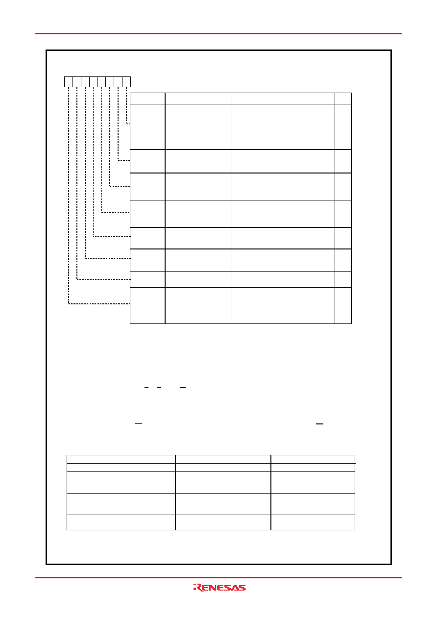
Three-phase PWM control register 0 (Note 1)
Symbol
Address
After reset
INVC0
034816
0016
b7 b6 b5 b4 b3 b2 b1 b0
Effective interrupt output
polarity select bit
INV00
Bit symbol
Bit name
Description
RW
INV01
Effective interrupt output
specification bit
INV02
Mode select bit
INV04
Positive and negative
phases concurrent output
disable bit
INV07
Software trigger select bit
INV06
Modulation mode select
bit
INV05
Positive and negative
phases concurrent output
detect flag
INV03
Output control bit
0: The ICTB2 counter is incremented by
one on the reising edge of the timer A1
reload control signal
1: The ICTB2 counter is incremented by
one on the falling edge of the timer A1
reload control signal
0: ICTB2 counter incremented by 1 at a
timer B2 underflow
1: Selected by INV00 bit
0: Three-phase motor control timer
function unused
1: Three-phase motor control timer
function
0: Three-phase motor control timer output
disabled
1: Three-phase motor control timer output
enabled
0: Simultaneous active output enabled
1: Simultaneous active output disabled
0: Not detected yet
1: Already detected
0: Triangular wave modulation mode
1: Sawtooth wave modulation mode
Setting this bit to “1” generates a transfer
trigger. If the INV06 bit is “1”, a trigger for
the dead time timer is also generated.
The value of this bit when read is “0”.
(Note 9)
(Note 3)
(Note 7)
(Note 2, Note 3)
Note 1: Write to this register after setting the PRC1 bit in the PRCR register to “1” (write enable). Note also that INV00 to INV02,
INV04 and INV06 bits can only be rewritten when timers A1, A2, A4 and B2 are idle.
Note 2: If this bit needs to be set to “1”, set any value in the ICTB2 register before writing to it.
Note 3: Effective when the INV11 bit is set to “1” (three-phase mode 1). If INV11 is set to “0” (three-phase mode 0), the ICTB2
counter is incremented by “1” each time the timer B2 underflows, regardless of whether the INV00 and INV01 bits are set.
When setting the INV01 bit to “1”, set the timer A1 count start flag before the first timer B2 underflow.
When the INV00 bit is set to “1”, the first interrupt is generated when the timer B2 underflows n-1 times, if n is the value set
in the ICTB2 counter. Subsequent interrupts are generated every n times the timer B2 underflow.
Note 4: Setting the INV02 bit to “1” activates the dead time timer, U/V/W-phase output control circuits and ICTB2 counter.
Note 5: When the INV02 bit is set to “1”(theee-phase control timer functions) and the INV03 is set to "0"(three-phase motor control
timer output disabled), U, U, V, V, W and W pins, including pins shared with other output functions, enter a high-
impedance state.
Note 6: The INV03 bit is set to “0” in the following cases:
When reset
When positive and negative go active (INV05="1") simultaneously while INV04 bit is set to “1”
When set to “0” in a program
When input on the SD pin changes state from “H” to “L” (The INV03 bit cannot be set to “1” when SD input is “L”.)
When both the INV04 and the INV05 bits are set to “1”, the INV03 bit is set to “0”.
Note 7: Can only be set by writing “0” in a program, and cannot be set to “1”.
Note 8: The effects of the INV06 bit are described in the table below.
(Note 4)
RW
(Note 5)
(Note 8)
Item
Mode
Timing at which transferred from IDB0 to
IDB1 registers to three-phase output shift
register
Timing at which dead time timer trigger is
generated when INV16 bit is “0”
INV13 bit
INV06=0
Triangular wave modulation mode
Transferred only once synchronously
with the transfer trigger after writing to
the IDB0 to IDB1 registers
Synchronous with the falling edge of
timer A1, A2, or A4 one-shot pulse
Effective when INV11 is “1” and INV06
is “0”
INV06=1
Sawtooth wave modulation mode
Transferred every transfer trigger
Synchronous with the transfer
trigger and the falling edge of timer
A1, A2, or A4 one-shot pulse
Transfer trigger: Timer B2 underflow, write to the INV07 bit or write to the TB2 register when INV10 is “1”
Note 9: If the INV06 bit is “1”, set the INV11 bit to “0” (three-phase mode 0) and set the PWCON bit to “0” (timer B2
reloaded by a timer B2 underflow).
Note10: Individual pins can be disabled using PFCR register.
(Note 6)
Has no effect
(Note 10)
(Note 5)
Figure 12.3.2. INVC0 Register
相关PDF资料 |
PDF描述 |
|---|---|
| M30260F3AGP-U7 | 16-BIT, FLASH, 20 MHz, MICROCONTROLLER, PQFP48 |
| M30263F8AFP-U5 | 16-BIT, FLASH, 20 MHz, MICROCONTROLLER, PDSO42 |
| M30260F6AGP-U7 | 16-BIT, FLASH, 20 MHz, MICROCONTROLLER, PQFP48 |
| M30260F8AGP-U5 | 16-BIT, FLASH, 20 MHz, MICROCONTROLLER, PQFP48 |
| M30263F8AFP-U9 | 16-BIT, FLASH, 20 MHz, MICROCONTROLLER, PDSO42 |
相关代理商/技术参数 |
参数描述 |
|---|---|
| M30260F6AGP D3 | 制造商:Renesas Electronics Corporation 功能描述: |
| M30260F6AGP D5 | 制造商:Renesas Electronics Corporation 功能描述: |
| M30260F6AGP#D3 | 功能描述:IC M16C MCU FLASH 48K 48LQFP RoHS:否 类别:集成电路 (IC) >> 嵌入式 - 微控制器, 系列:M16C™ M16C/微型/26A 产品培训模块:MCU Product Line Introduction XMEGA Introduction AVR XMEGA USB Connectivity 标准包装:90 系列:AVR® XMEGA 核心处理器:AVR 芯体尺寸:8/16-位 速度:32MHz 连通性:I²C,IrDA,SPI,UART/USART 外围设备:欠压检测/复位,DMA,POR,PWM,WDT 输入/输出数:50 程序存储器容量:192KB(96K x 16) 程序存储器类型:闪存 EEPROM 大小:4K x 8 RAM 容量:16K x 8 电压 - 电源 (Vcc/Vdd):1.6 V ~ 3.6 V 数据转换器:A/D 16x12b; D/A 2x12b 振荡器型:内部 工作温度:-40°C ~ 85°C 封装/外壳:64-TQFP 包装:托盘 配用:ATSTK600-RC14-ND - STK600 SOCKET/ADAPTER 64TQFPATSTK600-TQFP64-ND - STK600 SOCKET/ADAPTER 64-TQFPATAVRONEKIT-ND - KIT AVR/AVR32 DEBUGGER/PROGRMMRATAVRISP2-ND - PROGRAMMER AVR IN SYSTEM |
| M30260F6AGP#U3 | 功能描述:IC M16C MCU FLASH 48K 48LQFP RoHS:是 类别:集成电路 (IC) >> 嵌入式 - 微控制器, 系列:M16C™ M16C/微型/26A 标准包装:250 系列:56F8xxx 核心处理器:56800E 芯体尺寸:16-位 速度:60MHz 连通性:CAN,SCI,SPI 外围设备:POR,PWM,温度传感器,WDT 输入/输出数:21 程序存储器容量:40KB(20K x 16) 程序存储器类型:闪存 EEPROM 大小:- RAM 容量:6K x 16 电压 - 电源 (Vcc/Vdd):2.25 V ~ 3.6 V 数据转换器:A/D 6x12b 振荡器型:内部 工作温度:-40°C ~ 125°C 封装/外壳:48-LQFP 包装:托盘 配用:MC56F8323EVME-ND - BOARD EVALUATION MC56F8323 |
| M30260F6AGP#U3A | 功能描述:IC M16C/26A MCU FLASH 48K 48LQFP RoHS:是 类别:集成电路 (IC) >> 嵌入式 - 微控制器, 系列:M16C™ M16C/微型/26A 标准包装:1 系列:87C 核心处理器:MCS 51 芯体尺寸:8-位 速度:16MHz 连通性:SIO 外围设备:- 输入/输出数:32 程序存储器容量:8KB(8K x 8) 程序存储器类型:OTP EEPROM 大小:- RAM 容量:256 x 8 电压 - 电源 (Vcc/Vdd):4 V ~ 6 V 数据转换器:- 振荡器型:外部 工作温度:0°C ~ 70°C 封装/外壳:44-DIP 包装:管件 其它名称:864285 |
发布紧急采购,3分钟左右您将得到回复。