- 您现在的位置:买卖IC网 > PDF目录45012 > M30260F8AGP 16-BIT, FLASH, 20 MHz, MICROCONTROLLER, PQFP48 PDF资料下载
参数资料
| 型号: | M30260F8AGP |
| 元件分类: | 微控制器/微处理器 |
| 英文描述: | 16-BIT, FLASH, 20 MHz, MICROCONTROLLER, PQFP48 |
| 封装: | 7 X 7 MM, 0.50 MM PITCH, PLASTIC, LQFP-48 |
| 文件页数: | 9/30页 |
| 文件大小: | 311K |
| 代理商: | M30260F8AGP |
第1页第2页第3页第4页第5页第6页第7页第8页当前第9页第10页第11页第12页第13页第14页第15页第16页第17页第18页第19页第20页第21页第22页第23页第24页第25页第26页第27页第28页第29页第30页
1. Overview
page 15
6
2
f
o
6
0
2
,
5
2
.
l
u
J
1
5
.
0
.
v
e
R
1
5
0
-
1
7
0
B
3
0
J
E
R
)
T
6
2
/
C
6
1
M
,
B
6
2
/
C
6
1
M
,
A
6
2
/
C
6
1
M
(
p
u
o
r
G
A
6
2
/
C
6
1
M
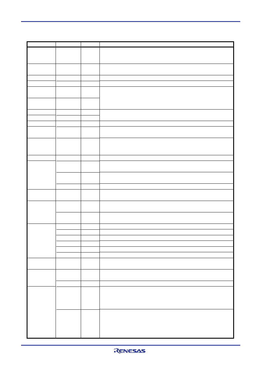
1.6 Pin Description
Apply 0V to the Vss pin. Apply following voltage to the Vcc pin.
2.7 to 5.5 V (M16C/26A, M16C/26B), 3.0 to 5.5 V (M16C/26T T-ver.), 4.2
to 5.5 V (M16C/26T V-ver.)
Supplies power to the A/D converter. Connect the AVCC pin to VCC and
the AVSS pin to VSS
___________
The MCU is in a reset state when "L" is applied to the RESET pin
Connect the CNVSS pin to VSS
I/O pins for the main clock oscillation circuit. Connect a ceramic resonator
or crystal oscillator between XIN and XOUT. To apply external clock, apply
it to XIN and leave XOUT open. If XIN is not used (for external oscillator or
external clock), connect XIN pin to VCC and leave XOUT open
I/O pins for the sub clock oscillation circuit. Connect a crystal oscillator
between XCIN and XCOUT
Outputs the clock having the same frequency as f1, f8, f32, or fC
______
________
Input pins for the INT interrupt. INT2 can be used for Timer A Z-phase
function
_______
NMI
interrupt input pin. NMI cannot be used as I/O port while the three-phase
_______
motor control is enabled. Apply a stable "H" to NMI after setting it's direction
register to "0" when the three-phase motor control is enabled
Input pins for the key input interrupt
I/O pins for the timer A0 to A4
Input pins for the timer A0 to A4
Input pin for Z-phase
Timer B0 to B1 input pins
Output pins for the three-phase motor control timer
I/O pins for the three-phase motor control timer
Input pins to control data transmission
Output pins to control data reception
Inputs and outputs the transfer clock
Inputs serial data
Outputs serial data
Output pin for transfer clock
Applies reference voltage to the A/D converter
Analog input pins for the A/D converter
Input pin for an external A/D trigger
I/O ports for CMOS. Each port can be programmed for input or output
under the control of the direction register. An input port can be set, by
program, for a pull-up resistor available or for no pull-up resister available
in 3-bit units
I/O ports for CMOS. Each port can be programmed for input or output
under the control of the direction register. An input port can be set, by
program, for a pull-up resistor available or for no pull-up resister available
in 4-bit units
VCC, VSS
AVCC
AVSS
____________
RESET
CNVSS
XIN
XOUT
XCIN
XCOUT
CLKOUT
________
INT0 to INT5
_______
NMI
_____
KI0 to KI3
TA0OUT to
TA4OUT
TA0IN to
TA4IN
ZP
TB0IN to
TB1IN
___
U, U, V, V,
___
W, W
IDU, IDW,
_____
IDV, SD
_________
CTS1 to CTS2
_________
RTS1 to RTS2
CLK1 to CLK2
RxD1 to RxD2
TxD1 to TxD2
CLKS1
VREF
AN0 to AN7
AN30 to AN31
___________
ADTRG
P15 to P17
P64 to P67
P70 to P77
P80 to P87
P100 to P107
P90 to P91
Power Supply
Analog Power
Supply
Reset Input
CNVSS
Main Clock
Input
Main Clock
Output
Sub Clock Input
Sub Clock Output
Clock Output
______
INT Interrupt
Input
_______
NMI Interrupt
Input
Key Input Interrupt
Timer A
Timer B
Three-Phase
Motor Control
Timer Output
Serial I/O
Reference
Voltage Input
A/D Converter
I/O Ports
I
O
I
O
I
I/O
I
O
I/O
I
O
I/O
I
O
I
I/O
I : Input
O : Output
I/O : Input and output
Classification
Pin Name
I/O Type
Description
Table 1.13 Pin Description (48-Pin and 42-Pin Packages)
相关PDF资料 |
PDF描述 |
|---|---|
| M30260F6TGP | 16-BIT, FLASH, 20 MHz, MICROCONTROLLER, PQFP48 |
| M30260F6AGP | 16-BIT, FLASH, 20 MHz, MICROCONTROLLER, PQFP48 |
| M30263M4A-XXXFP-D5 | 16-BIT, MROM, 20 MHz, MICROCONTROLLER, PDSO42 |
| M30260F4VGP | 16-BIT, FLASH, 20 MHz, MICROCONTROLLER, PQFP48 |
| M30263F6AFP-D5 | 16-BIT, FLASH, 20 MHz, MICROCONTROLLER, PDSO42 |
相关代理商/技术参数 |
参数描述 |
|---|---|
| M30260F8AGP D3 | 制造商:Renesas Electronics Corporation 功能描述: |
| M30260F8AGP D5 | 制造商:Renesas Electronics Corporation 功能描述: |
| M30260F8AGP#D3 | 功能描述:MCU 3/5V 64K I-TEMP 48-LQFP RoHS:否 类别:集成电路 (IC) >> 嵌入式 - 微控制器, 系列:M16C™ M16C/微型/26A 标准包装:250 系列:56F8xxx 核心处理器:56800E 芯体尺寸:16-位 速度:60MHz 连通性:CAN,SCI,SPI 外围设备:POR,PWM,温度传感器,WDT 输入/输出数:21 程序存储器容量:40KB(20K x 16) 程序存储器类型:闪存 EEPROM 大小:- RAM 容量:6K x 16 电压 - 电源 (Vcc/Vdd):2.25 V ~ 3.6 V 数据转换器:A/D 6x12b 振荡器型:内部 工作温度:-40°C ~ 125°C 封装/外壳:48-LQFP 包装:托盘 配用:MC56F8323EVME-ND - BOARD EVALUATION MC56F8323 |
| M30260F8AGP#D5 | 功能描述:IC M16C MCU FLASH 64K 48-LQFP RoHS:否 类别:集成电路 (IC) >> 嵌入式 - 微控制器, 系列:M16C™ M16C/微型/26A 产品培训模块:MCU Product Line Introduction XMEGA Introduction AVR XMEGA USB Connectivity 标准包装:90 系列:AVR® XMEGA 核心处理器:AVR 芯体尺寸:8/16-位 速度:32MHz 连通性:I²C,IrDA,SPI,UART/USART 外围设备:欠压检测/复位,DMA,POR,PWM,WDT 输入/输出数:50 程序存储器容量:192KB(96K x 16) 程序存储器类型:闪存 EEPROM 大小:4K x 8 RAM 容量:16K x 8 电压 - 电源 (Vcc/Vdd):1.6 V ~ 3.6 V 数据转换器:A/D 16x12b; D/A 2x12b 振荡器型:内部 工作温度:-40°C ~ 85°C 封装/外壳:64-TQFP 包装:托盘 配用:ATSTK600-RC14-ND - STK600 SOCKET/ADAPTER 64TQFPATSTK600-TQFP64-ND - STK600 SOCKET/ADAPTER 64-TQFPATAVRONEKIT-ND - KIT AVR/AVR32 DEBUGGER/PROGRMMRATAVRISP2-ND - PROGRAMMER AVR IN SYSTEM |
| M30260F8AGP#D7 | 制造商:Renesas Electronics Corporation 功能描述:MCU 16BIT R8C CISC 64KB FLASH 3.3V/5V 48LQFP - Trays |
发布紧急采购,3分钟左右您将得到回复。