- 您现在的位置:买卖IC网 > PDF目录80531 > M30302MEP-XXXFP 16-BIT, MROM, 16 MHz, MICROCONTROLLER, PQFP100 PDF资料下载
参数资料
| 型号: | M30302MEP-XXXFP |
| 元件分类: | 微控制器/微处理器 |
| 英文描述: | 16-BIT, MROM, 16 MHz, MICROCONTROLLER, PQFP100 |
| 封装: | 14 X 20 MM, 0.65 MM PITCH, LEAD FREE, PLASTIC, LQFP-100 |
| 文件页数: | 4/57页 |
| 文件大小: | 649K |
| 代理商: | M30302MEP-XXXFP |
第1页第2页第3页当前第4页第5页第6页第7页第8页第9页第10页第11页第12页第13页第14页第15页第16页第17页第18页第19页第20页第21页第22页第23页第24页第25页第26页第27页第28页第29页第30页第31页第32页第33页第34页第35页第36页第37页第38页第39页第40页第41页第42页第43页第44页第45页第46页第47页第48页第49页第50页第51页第52页第53页第54页第55页第56页第57页
1. Overview
Page 12 of 53
1.6
Pin Description
I : Input
O : Output
I/O : Input and output
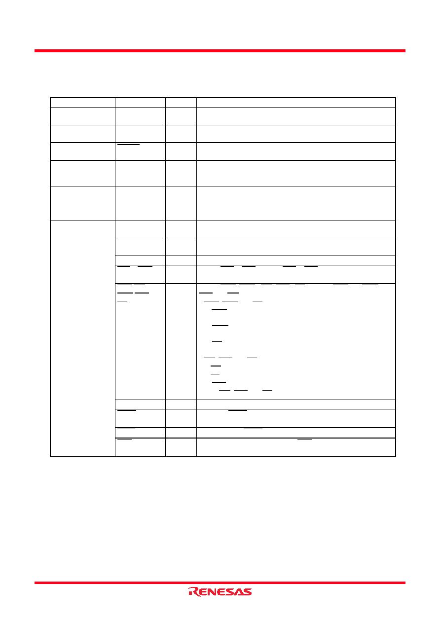
Table 1.8
Pin Description (1)
Signal Name
Pin Name
I/O Type
Description
Power supply input
VCC1, VCC2
VSS
I
Apply 2.7 to 5.5 V to the VCC1 and VCC2 pins and 0 V to the VSS
pin. The VCC apply condition is that VCC1 = VCC2.
Analog power
supply input
AVCC
AVSS
I
Applies the power supply for the A/D converter. Connect the AVCC
pin to VCC1. Connect the AVSS pin to VSS.
Reset input
RESET
I
The microcomputer is in a reset state when applying “L” to the this
pin.
CNVSS
I
Switches processor mode. Connect this pin to VSS to when after
a reset to start up in single-chip mode. Connect this pin to VCC1 to
start up in microprocessor mode.
External data bus
width select input
BYTE
I
Switches the data bus in external memory space. The data bus is
16 bits long when the this pin is held "L" and 8 bits long when the
this pin is held "H". Set it to either one. Connect this pin to VSS
when an single-chip mode.
Bus control pins
D0 to D7
I/O
Inputs and outputs data (D0 to D7) when these pins are set as the
separate bus.
D8 to D15
I/O
Inputs and outputs data (D8 to D15) when external 16-bit data bus
is set as the separate bus.
A0 to A19
O
Output address bits (A0 to A19).
CS0 to CS3
O
Output CS0 to CS3 signals. CS0 to CS3 are chip-select signals to
specify an external space.
WRL/WR
WRH/BHE
RD
O
Output WRL, WRH, (WR, BHE), RD signals. WRL and WRH or
BHE and WR can be switched by program.
WRL, WRH and RD are selected
The WRL signal becomes "L" by writing data to an even address in
an external memory space.
The WRH signal becomes "L" by writing data to an odd address in
an external memory space.
The RD pin signal becomes "L" by reading data in an external
memory space.
WR, BHE and RD are selected
The WR signal becomes "L" by writing data in an external memory space.
The RD signal becomes "L" by reading data in an external memory space.
The BHE signal becomes "L" by accessing an odd address.
Select WR, BHE and RD for an external 8-bit data bus.
ALE
O
ALE is a signal to latch the address.
HOLD
I
While the HOLD pin is held "L", the microcomputer is placed in a
hold state.
HLDA
O
In a hold state, HLDA outputs a "L" signal.
RDY
I
While applying a "L" signal to the RDY pin, the microcomputer is
placed in a wait state.
相关PDF资料 |
PDF描述 |
|---|---|
| MPC8378ECVRAGDA | 32-BIT, 266 MHz, MICROPROCESSOR, PBGA689 |
| MB90587CPMC | MICROCONTROLLER, PQFP100 |
| MB95F212HPH-G-SNE2 | MICROCONTROLLER, PDIP8 |
| MB95F213HPH-G-SNE2 | MICROCONTROLLER, PDIP8 |
| MC9S08SH8MTGR | MICROCONTROLLER, PDSO16 |
相关代理商/技术参数 |
参数描述 |
|---|---|
| M30302MEP-XXXGP | 制造商:RENESAS 制造商全称:Renesas Technology Corp 功能描述:SINGLE-CHIP 16-BIT CMOS MICROCOMPUTER |
| M30302SPFP | 制造商:RENESAS 制造商全称:Renesas Technology Corp 功能描述:SINGLE-CHIP 16-BIT CMOS MICROCOMPUTER |
| M30302SPFP#U3 | 功能描述:IC M16C/30P MCU ROMLESS 100QFP RoHS:是 类别:集成电路 (IC) >> 嵌入式 - 微控制器, 系列:M16C™ M16C/30 标准包装:250 系列:80C 核心处理器:8051 芯体尺寸:8-位 速度:16MHz 连通性:EBI/EMI,I²C,UART/USART 外围设备:POR,PWM,WDT 输入/输出数:40 程序存储器容量:- 程序存储器类型:ROMless EEPROM 大小:- RAM 容量:256 x 8 电压 - 电源 (Vcc/Vdd):4.5 V ~ 5.5 V 数据转换器:A/D 8x10b 振荡器型:内部 工作温度:-40°C ~ 85°C 封装/外壳:68-LCC(J 形引线) 包装:带卷 (TR) |
| M30302SPFP#U5 | 功能描述:MCU 3/5V 0K 100-QFP RoHS:是 类别:集成电路 (IC) >> 嵌入式 - 微控制器, 系列:M16C™ M16C/30 标准包装:250 系列:80C 核心处理器:8051 芯体尺寸:8-位 速度:16MHz 连通性:EBI/EMI,I²C,UART/USART 外围设备:POR,PWM,WDT 输入/输出数:40 程序存储器容量:- 程序存储器类型:ROMless EEPROM 大小:- RAM 容量:256 x 8 电压 - 电源 (Vcc/Vdd):4.5 V ~ 5.5 V 数据转换器:A/D 8x10b 振荡器型:内部 工作温度:-40°C ~ 85°C 封装/外壳:68-LCC(J 形引线) 包装:带卷 (TR) |
| M30302SPGP | 制造商:RENESAS 制造商全称:Renesas Technology Corp 功能描述:SINGLE-CHIP 16-BIT CMOS MICROCOMPUTER |
发布紧急采购,3分钟左右您将得到回复。