- 您现在的位置:买卖IC网 > PDF目录80446 > M30620FCPGP-D9 16-BIT, FLASH, 24 MHz, MICROCONTROLLER, PQFP100 PDF资料下载
参数资料
| 型号: | M30620FCPGP-D9 |
| 元件分类: | 微控制器/微处理器 |
| 英文描述: | 16-BIT, FLASH, 24 MHz, MICROCONTROLLER, PQFP100 |
| 封装: | 14 X 14 MM, 0.50 MM PITCH, PLASTIC, LQFP-100 |
| 文件页数: | 27/87页 |
| 文件大小: | 919K |
| 代理商: | M30620FCPGP-D9 |
第1页第2页第3页第4页第5页第6页第7页第8页第9页第10页第11页第12页第13页第14页第15页第16页第17页第18页第19页第20页第21页第22页第23页第24页第25页第26页当前第27页第28页第29页第30页第31页第32页第33页第34页第35页第36页第37页第38页第39页第40页第41页第42页第43页第44页第45页第46页第47页第48页第49页第50页第51页第52页第53页第54页第55页第56页第57页第58页第59页第60页第61页第62页第63页第64页第65页第66页第67页第68页第69页第70页第71页第72页第73页第74页第75页第76页第77页第78页第79页第80页第81页第82页第83页第84页第85页第86页第87页
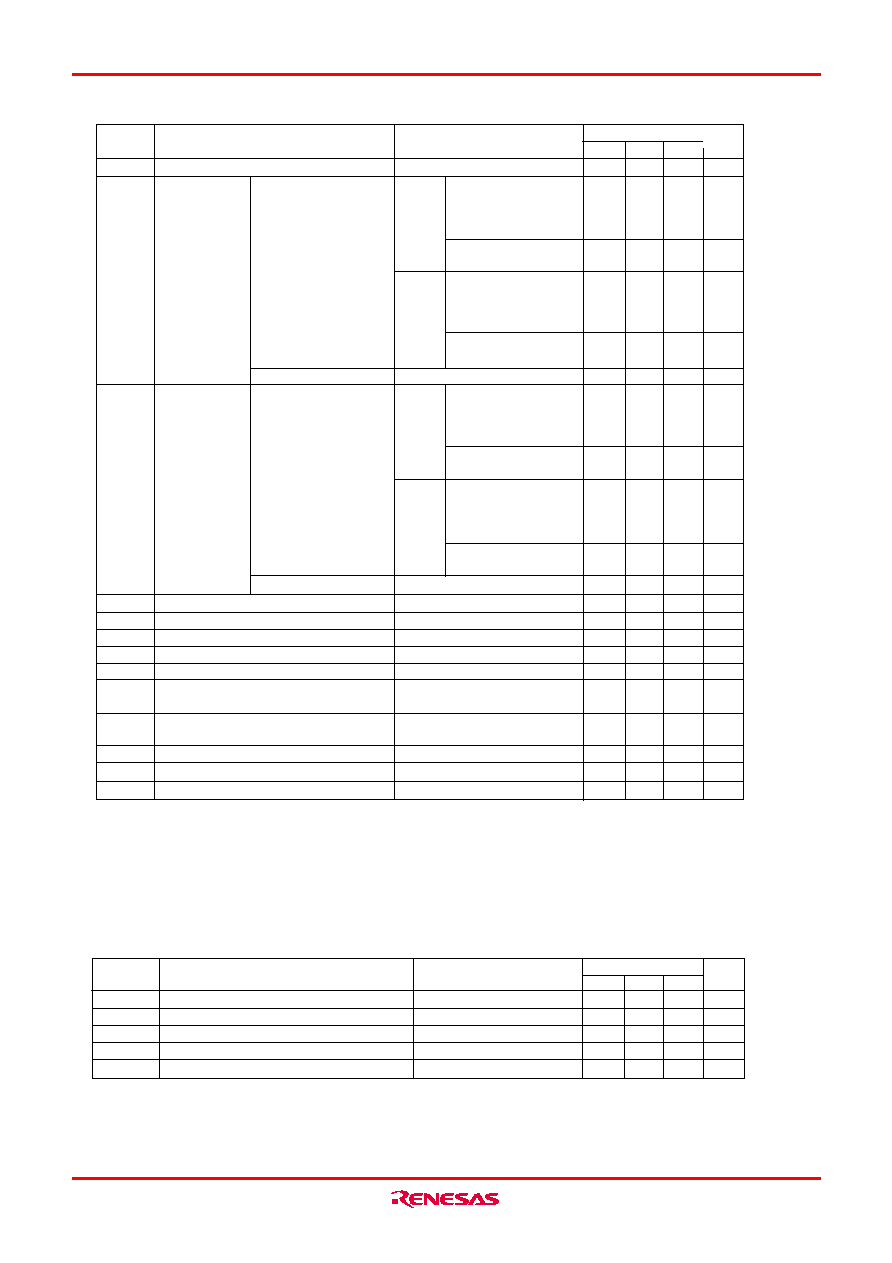
M16C/62P Group (M16C/62P, M16C/62PT)
5. Electrical Characteristics (M16C/62P)
4
8
f
o
4
0
2
,
1
0
p
e
S
0
3
.
2
.
v
e
R
Z
0
3
2
0
-
1
0
B
3
0
J
E
R
page 33
Table 5.3 A/D Conversion Characteristics (1)
Standard
Min.
Typ.Max.
–
INL
Resolution
Integral
Non-Linearity
Error
Bits
VREF =VCC1
10
SymbolParameter
Measuring Condition
Unit
AN0 to AN7 input
AN0_0 to AN0_7 input
AN2_0 to AN2_7 input
ANEX0, ANEX1 input
VREF=
VCC1=
5V
LSB
±3
LSB
±7
LSB
VREF =VCC1=3.3V
8 bits
±2
RLADDER
tCONV
Ladder Resistance
10-bit Conversion Time, Sample & Hold
Function Available
Reference Voltage
Analog Input Voltage
k
s
V
VIA
VREF
V
0
2.0
10
VCC1
VREF
40
2.75
8-bit Conversion Time, Sample & Hold
Function Available
s
2.33
tCONV
tSAMP
Sampling Time0.25
s
VREF =VCC1
VREF =VCC1=5V, AD=12MHz
VREF =VCC1=5V, AD=12MHz
DNL
Differential Non-Linearity Error
Offset Error
Gain Error
–
LSB
±1
±3
NOTES:
1. Referenced to VCC1=AVCC=VREF=3.3 to 5.5V, VSS=AVSS=0V at Topr = -20 to 85
°C / -40 to 85 °C unless otherwise
specified.
2. If VCC1 > VCC2, do not use AN0_0 to AN0_7 and AN2_0 to AN2_7 as analog input pins.
3. AD frequency must be 12 MHz or less. And divide the fAD if VCC1 is less than 4.0V, and AD frequency into 10 MHz
or less.
4. When sample & hold function is disabled, AD frequency must be 250 kHz or more, in addition to the limitation in Note 3.
When sample & hold function is enabled, AD frequency must be 1MHz or more, in addition to the limitation in Note 3.
10 bits
VREF=
VCC1=
3.3V
LSB
±5
LSB
±7
VREF=
VCC1=
5V
LSB
±3
LSB
±7
LSB
VREF =VCC1=3.3V
8 bits
±2
10 bits
VREF=
VCC1=
3.3V
LSB
±5
LSB
±7
–
Absolute
Accuracy
External operation amp
connection mode
AN0 to AN7 input
AN0_0 to AN0_7 input
AN2_0 to AN2_7 input
ANEX0, ANEX1 input
External operation amp
connection mode
AN0 to AN7 input
AN0_0 to AN0_7 input
AN2_0 to AN2_7 input
ANEX0, ANEX1 input
External operation amp
connection mode
AN0 to AN7 input
AN0_0 to AN0_7 input
AN2_0 to AN2_7 input
ANEX0, ANEX1 input
External operation amp
connection mode
Tolerance Level Impedance
–
3k
Table 5.4 D/A Conversion Characteristics (1)
Min.
Typ.Max.
–
tsu
RO
Resolution
Absolute Accuracy
Setup Time
Output Resistance
Reference Power Supply Input Current
Bits
%
k
mA
IVREF
1.0
1.5
8
3
Symbol
Parameter
Measuring Condition
Unit
20
10
4
s
(NOTE 2)
Standard
NOTES:
1. Referenced to VCC1=VREF=3.3 to 5.5V, VSS=AVSS=0V at Topr = -20 to 85
°C / -40 to 85 °C unless otherwise specified.
2. This applies when using one D/A converter, with the D/A register for the unused D/A converter set to “00h”. The
resistor ladder of the A/D converter is not included. Also, when D/A register contents are not “00h,” the IVREF will
flow even if Vref is disconnected by the A/D control register.
相关PDF资料 |
PDF描述 |
|---|---|
| M3062CF8TFP-B7 | 16-BIT, FLASH, 24 MHz, MICROCONTROLLER, PQFP100 |
| MC68HC711N4VFS2 | 8-BIT, UVPROM, 2 MHz, MICROCONTROLLER, CQCC84 |
| MPC852TCZT66A | 32-BIT, 66 MHz, RISC PROCESSOR, PBGA256 |
| MC9S08JS8LCFK | MICROCONTROLLER, QCC24 |
| MC9S12GC16CPB | 16-BIT, FLASH, 25 MHz, MICROCONTROLLER, PQFP52 |
相关代理商/技术参数 |
参数描述 |
|---|---|
| M30620FCPGPU5C | 制造商:Renesas Electronics Corporation 功能描述:MCU,M16C/62P Group (M16C/62P, M16C/62PT) |
| M30620M8-359FP | 制造商:MITSUBISHI 制造商全称:Mitsubishi Electric Semiconductor 功能描述:SINGLE-CHIP 16-BIT CMOS MICROCOMPUTER |
| M30620M8-A69GP | 制造商:MITSUBISHI 制造商全称:Mitsubishi Electric Semiconductor 功能描述:SINGLE-CHIP 16-BIT CMOS MICROCOMPUTER |
| M30620M8A-C11GP#U0 | 制造商:Renesas Electronics Corporation 功能描述: |
| M30620M8A-XXXFP | 制造商:MITSUBISHI 制造商全称:Mitsubishi Electric Semiconductor 功能描述:SINGLE-CHIP 16-BIT CMOS MICROCOMPUTER |
发布紧急采购,3分钟左右您将得到回复。