- 您现在的位置:买卖IC网 > PDF目录45018 > M30623ECVGP 16-BIT, OTPROM, 16 MHz, MICROCONTROLLER, PQFP80 PDF资料下载
参数资料
| 型号: | M30623ECVGP |
| 元件分类: | 微控制器/微处理器 |
| 英文描述: | 16-BIT, OTPROM, 16 MHz, MICROCONTROLLER, PQFP80 |
| 封装: | PLASTIC, QFP-80 |
| 文件页数: | 107/187页 |
| 文件大小: | 2666K |
| 代理商: | M30623ECVGP |
第1页第2页第3页第4页第5页第6页第7页第8页第9页第10页第11页第12页第13页第14页第15页第16页第17页第18页第19页第20页第21页第22页第23页第24页第25页第26页第27页第28页第29页第30页第31页第32页第33页第34页第35页第36页第37页第38页第39页第40页第41页第42页第43页第44页第45页第46页第47页第48页第49页第50页第51页第52页第53页第54页第55页第56页第57页第58页第59页第60页第61页第62页第63页第64页第65页第66页第67页第68页第69页第70页第71页第72页第73页第74页第75页第76页第77页第78页第79页第80页第81页第82页第83页第84页第85页第86页第87页第88页第89页第90页第91页第92页第93页第94页第95页第96页第97页第98页第99页第100页第101页第102页第103页第104页第105页第106页当前第107页第108页第109页第110页第111页第112页第113页第114页第115页第116页第117页第118页第119页第120页第121页第122页第123页第124页第125页第126页第127页第128页第129页第130页第131页第132页第133页第134页第135页第136页第137页第138页第139页第140页第141页第142页第143页第144页第145页第146页第147页第148页第149页第150页第151页第152页第153页第154页第155页第156页第157页第158页第159页第160页第161页第162页第163页第164页第165页第166页第167页第168页第169页第170页第171页第172页第173页第174页第175页第176页第177页第178页第179页第180页第181页第182页第183页第184页第185页第186页第187页
26
Mitsubishi microcomputers
M16C / 62T Group
SINGLE-CHIP 16-BIT CMOS MICROCOMPUTER
Memory Space Expansion Functions
The data bank register is made up of the bank selection bits (bits 5 through 3) and the offset bit (bit 2). The
bank selection bits are used to set a bank number for accessing data lying between 4000016 and
BFFFF16. Assigning 1 to the offset bit provides the means to set offsets covering 4000016.
Figure 1.8.5 shows the memory location and chip select areas in expansion mode 2.
_______
The area relevant to CS0 ranges from 4000016 through FFFFF16. As for the area from 4000016 through
_______
BFFFF16, the bank number set by use of the bank selection bits are output from the output terminals CS3
_______
- CS1 only in accessing data. In fetching a program, bank 7 (1112) is output from CS3 - CS1. As for the
_______
area from C000016 through FFFFF16, bank 7 (1112) is output from CS3 - CS1 without regard to accessing
data or to fetching a program.
_______
In accessing an area irrelevant to CS0, a chip select signal CS3 (400016 - 7FFF16), CS2 (800016 -
_______
27FFF16), and CS1 (2800016 - 3FFFF16) is output depending on the address as in the past.
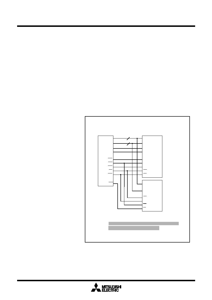
Figure 1.8.6 shows an example of connecting the MCU with a 4-M byte ROM and to a 128-K byte SRAM.
_______
Connect the chip select of 4-M byte ROM with CS0. Connect M16C’s CS3, CS2, and CS1 with address
inputs AD21, AD20, and A19 respectively. Connect M16C’s output AD19 with address input AD18. Fig-
ure 1.8.7 shows the relationship between addresses of the 4-M byte ROM and those of M16C.
An example of connecting the MCU with
external memories in expansion mode 2
(M30622MC, Microprocessor mode)
17
8
M30622MCT-XXXFP
D0 to D7
A0 to A16
A17
RD
WR
CS1
CS2
CS3
CS0
A19
4-M
byte
ROM
DQ0 to DQ7
AD0 to AD16
AD17
AD18
AD19
OE
CS
128-K
byte
SRAM
DQ0 to DQ7
AD0 to AD16
S2
W
OE
S1
AD20
AD21
Note 1. If only one chip select terminal (S1 or S2) is present,
decoding by use of an external circuit is required.
Note 2. M30623(80-pin package) is not provided with the
output pin for the chip select signal.
Note 3. The M16C/62T group is not guaranteed to operate
in memory expansion and microprocessor modes.
In this mode, memory is banked
every 512 K bytes, so that data
access in different banks requires
switching over banks. However,
data on bank boundaries when
offset bit = 0 can be accessed
successively by setting the offset
bit to 1, because in which case
the memory address is offset by
4000016. For example, two bytes
of data located at addresses
0FFFFF16 and 10000016 of 4-
Mbyte ROM can be accessed
successively without having to
change the bank bit by setting the
offset bit to 1 and then accessing
addresses 07FFFF 16 and
80000016.
On the other hand, the SRAM’s
_______
chip select assumes that CS0=1
_______
(not selected) and CS2=0 (se-
_______
lected), so connect CS0 with S2
_______
____
and CS2 with S1. If the SRAM
doesn’t have a bipolar chip select
_______
input terminal, decode CS0 and
_______
CS2 externally.
Figure 1.8.6. An example of connecting the MCU with
external memories in expansion mode 2
相关PDF资料 |
PDF描述 |
|---|---|
| M30622ECV-XXXFP | 16-BIT, OTPROM, 16 MHz, MICROCONTROLLER, PQFP100 |
| M30622ECT-XXXFP | 16-BIT, OTPROM, 16 MHz, MICROCONTROLLER, PQFP100 |
| M30623ECTGP | 16-BIT, OTPROM, 16 MHz, MICROCONTROLLER, PQFP80 |
| M30623MCV-XXXGP | 16-BIT, MROM, 16 MHz, MICROCONTROLLER, PQFP80 |
| M30623M8T-XXXGP | 16-BIT, MROM, 16 MHz, MICROCONTROLLER, PQFP80 |
相关代理商/技术参数 |
参数描述 |
|---|---|
| M30623EG | 制造商:RENESAS 制造商全称:Renesas Technology Corp 功能描述:SINGLE-CHIP 16-BIT CMOS MICROCOMPUTER |
| M30623F4 | 制造商:RENESAS 制造商全称:Renesas Technology Corp 功能描述:SINGLE-CHIP 16-BIT CMOS MICROCOMPUTER |
| M30623F8 | 制造商:RENESAS 制造商全称:Renesas Technology Corp 功能描述:SINGLE-CHIP 16-BIT CMOS MICROCOMPUTER |
| M30623F8PGP | 制造商:RENESAS 制造商全称:Renesas Technology Corp 功能描述:SINGLE-CHIP 16-BIT CMOS MICROCOMPUTER |
| M30623F8PGP#D3C | 功能描述:MCU 3/5V 64K I-TEMP 80-QFP RoHS:否 类别:集成电路 (IC) >> 嵌入式 - 微控制器, 系列:M16C™ M16C/60/62P 标准包装:250 系列:56F8xxx 核心处理器:56800E 芯体尺寸:16-位 速度:60MHz 连通性:CAN,SCI,SPI 外围设备:POR,PWM,温度传感器,WDT 输入/输出数:21 程序存储器容量:40KB(20K x 16) 程序存储器类型:闪存 EEPROM 大小:- RAM 容量:6K x 16 电压 - 电源 (Vcc/Vdd):2.25 V ~ 3.6 V 数据转换器:A/D 6x12b 振荡器型:内部 工作温度:-40°C ~ 125°C 封装/外壳:48-LQFP 包装:托盘 配用:MC56F8323EVME-ND - BOARD EVALUATION MC56F8323 |
发布紧急采购,3分钟左右您将得到回复。