- 您现在的位置:买卖IC网 > PDF目录80478 > M30623MAA-XXXGP 16-BIT, MROM, 16 MHz, MICROCONTROLLER, PQFP80 PDF资料下载
参数资料
| 型号: | M30623MAA-XXXGP |
| 元件分类: | 微控制器/微处理器 |
| 英文描述: | 16-BIT, MROM, 16 MHz, MICROCONTROLLER, PQFP80 |
| 封装: | 14 X 14 MM, 0.65 MM PITCH, PLASTIC, QFP-80 |
| 文件页数: | 22/143页 |
| 文件大小: | 3168K |
| 代理商: | M30623MAA-XXXGP |
第1页第2页第3页第4页第5页第6页第7页第8页第9页第10页第11页第12页第13页第14页第15页第16页第17页第18页第19页第20页第21页当前第22页第23页第24页第25页第26页第27页第28页第29页第30页第31页第32页第33页第34页第35页第36页第37页第38页第39页第40页第41页第42页第43页第44页第45页第46页第47页第48页第49页第50页第51页第52页第53页第54页第55页第56页第57页第58页第59页第60页第61页第62页第63页第64页第65页第66页第67页第68页第69页第70页第71页第72页第73页第74页第75页第76页第77页第78页第79页第80页第81页第82页第83页第84页第85页第86页第87页第88页第89页第90页第91页第92页第93页第94页第95页第96页第97页第98页第99页第100页第101页第102页第103页第104页第105页第106页第107页第108页第109页第110页第111页第112页第113页第114页第115页第116页第117页第118页第119页第120页第121页第122页第123页第124页第125页第126页第127页第128页第129页第130页第131页第132页第133页第134页第135页第136页第137页第138页第139页第140页第141页第142页第143页
Mitsubishi microcomputers
M16C / 62A Group (80-pin)
SINGLE-CHIP 16-BIT CMOS MICROCOMPUTER
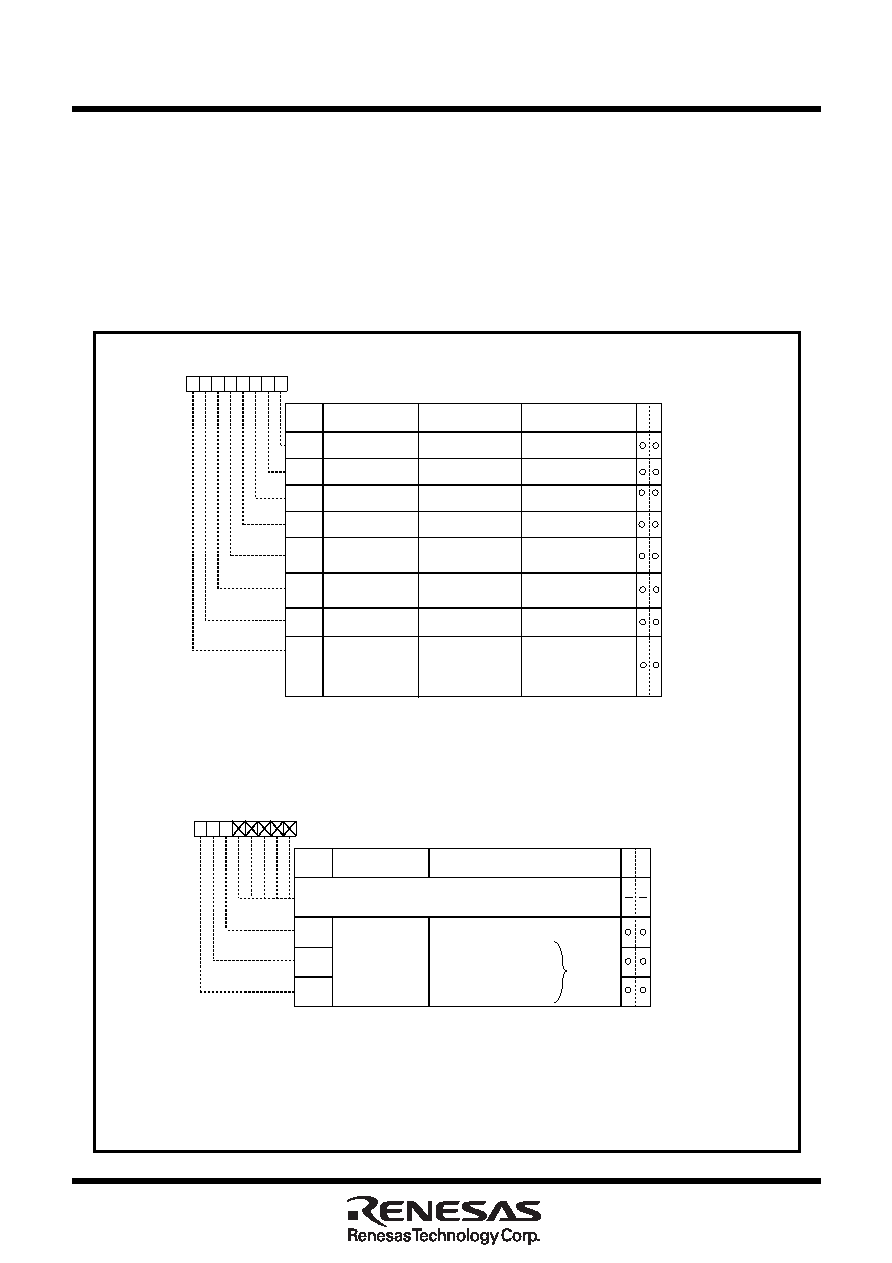
UART2 Special Mode Register
115
UART2 Special Mode Register
The UART2 special mode register (address 037716) is used to control UART2 in various ways.
Figure 1.14.25 shows the UART2 special mode register.
Bit 0 of the UART2 special mode register (037716) is used as the I2C mode select bit.
Setting “1” in the I2C mode select bit (bit 0) goes the circuit to achieve the I2C bus (simplified I2C bus)
interface effective.
Table 1.14.9 shows the relation between the I2C mode select bit and respective control workings.
Since this function uses clock-synchronous serial I/O mode, set this bit to “0” in UART mode.
Figure 1.14.25. UART2 special mode register
UART2 special mode register
Symbol
Address
When reset
U2SMR
037716
0016
b7
b6
b5
b4 b3
b2
b1
b0
Bit name
Bit
symbol
W
R
Function
(During UART mode)
Function
(During clock synchronous
serial I/O mode)
ABSCS
ACSE
SSS
I2C mode select bit
Bus busy flag
0 : STOP condition detected
1 : START condition detected
SCLL sync output
enable bit
Bus collision detect
sampling
clock select bit
Arbitration lost detecting
flag control bit
0 : Normal mode
1 : I2C mode
0 : Update per bit
1 : Update per byte
IICM
ABC
BBS
LSYN
0 : Ordinary
1 : Falling edge of RxD2
0 : Disabled
1 : Enabled
Transmit start condition
select bit
Must always be “0”
0 : Rising edge of transfer
clock
1 : Underflow signal of timer A0
Auto clear function
select bit of transmit
enable bit
0 : No auto clear function
1 : Auto clear at occurrence of
bus collision
Must always be “0”
Note 1: Nothing but “0” may be written.
Note 2: When not in I2C mode, do not set this bit by writing a “1”. During normal mode, set it to “0”. When this
bit = “0”, UART2 special mode register 3 (U2SMR3 at address 037516) bits 7 to 5 (DL2 to DL0 = SDA
digital delay setup bits) are initialized to “000”, with the analog delay circuit selected. Also, when SDDS
= “0”, the U2SMR3 register cannot be read or written to.
Note 3: When analog delay is selected, only the analog delay value is effective; when digital delay is selected,
only the digital delay value is effective.
(Note1)
SDDS
SDA digital delay select
bit (Note 2, Note 3)
Must always be “0”
0 : Analog delay output
is selected
1 : Digital delay output
is selected
(must always be “0” when
not using I C mode)
2
UART2 special mode register 3 (I C bus exclusive use register)
Symbol
Address
When reset
U2SMR3
037516
Indeterminate
(However, when SDDS = “1”, the initial value is “0016”)
b7
b6 b5
b4
b3
b2
b1
b0
Bit name
Bit
symbol
W
R
Function
(I C bus exclusive use register)
DL2
SDA digital delay setup
bit
(Note 1, Note 2, Note 3,
Note 4)
DL0
DL1
0 0 0 : Analog delay is selected
0 0 1 : 1 to 2 cycle(s) of 1/f(XIN)
0 1 0 : 2 to 3 cycles of 1/f(XIN)
0 1 1 : 3 to 4 cycles of 1/f(XIN)
1 0 0 : 4 to 5 cycles of 1/f(XIN)
1 0 1 : 5 to 6 cycles of 1/f(XIN)
1 1 0 : 6 to 7 cycles of 1/f(XIN)
1 1 1 : 7 to 8 cycles of 1/f(XIN)
2
Nothing is assigned.
In an attempt to write to these bits, write “0”. The value, if read, turns out to be
indeterminate. However, when SDDS = “1”, the value “0” is read out (Note 1)
2
b7 b6 b5
Note 1: This bit can be read or written to when UART2 special mode register (U2SMR at address 037716) bit
7 (SDDS: SDA digital delay select bit) = “1”. When the initial value of UART2 special mode register 3
(U2SMR3) is read after setting SDDS = “1”, the value is “0016”. When writing to UART2 special mode
register 3 (U2SMR3) after setting SDDS = “1”, be sure to write 0's to bits 0–4. When SDDS = “0”,
this register cannot be written to; when read, the value is indeterminate.
Note 2: These bits are initialized to “000” when SDDS = “0”, with the analog delay circuit selected. After a reset,
these bits are set to “000”, with the analog delay circuit selected. However, because these bits can be
read only when SDDS = “1”, the value read from these bits when SDDS = “0” is indeterminate.
Note 3: When analog delay is selected, only the analog delay value is effective; when digital delay is selected,
only the digital delay value is effective.
Note 4: The amount of delay varies with the load on SCL and SDA pins. Also, when using an external clock, the
amount of delay increases by about 100 ns, so be sure to take this into account when using the device.
Digital delay
is selected
相关PDF资料 |
PDF描述 |
|---|---|
| M30624FGMFP | 16-BIT, FLASH, 10 MHz, MICROCONTROLLER, PQFP100 |
| M30624FGPGP-U9 | 16-BIT, FLASH, 24 MHz, MICROCONTROLLER, PQFP100 |
| M30840MC-XXXFP | 32-BIT, MROM, 32 MHz, MICROCONTROLLER, PQFP100 |
| M30855FHTGP | 32-BIT, FLASH, 32 MHz, MICROCONTROLLER, PQFP144 |
| M32196F8TFP | 32-BIT, FLASH, 160 MHz, RISC MICROCONTROLLER, PQFP144 |
相关代理商/技术参数 |
参数描述 |
|---|---|
| M30623MAH-A81GP | 制造商:MITSUBISHI 制造商全称:Mitsubishi Electric Semiconductor 功能描述:SINGLE-CHIP 16-BIT CMOS MICROCOMPUTER |
| M30623MAP | 制造商:RENESAS 制造商全称:Renesas Technology Corp 功能描述:SINGLE-CHIP 16-BIT CMOS MICROCOMPUTER |
| M30623MAP-XXXGP | 制造商:RENESAS 制造商全称:Renesas Technology Corp 功能描述:SINGLE-CHIP 16-BIT CMOS MICROCOMPUTER |
| M30623MA-XXXGP | 制造商:RENESAS 制造商全称:Renesas Technology Corp 功能描述:SINGLE-CHIP 16-BIT CMOS MICROCOMPUTER |
| M30623MC | 制造商:RENESAS 制造商全称:Renesas Technology Corp 功能描述:SINGLE-CHIP 16-BIT CMOS MICROCOMPUTER |
发布紧急采购,3分钟左右您将得到回复。