- 您现在的位置:买卖IC网 > PDF目录45017 > M30624MGN-XXXGP 16-BIT, MROM, 16 MHz, MICROCONTROLLER, PQFP100 PDF资料下载
参数资料
| 型号: | M30624MGN-XXXGP |
| 元件分类: | 微控制器/微处理器 |
| 英文描述: | 16-BIT, MROM, 16 MHz, MICROCONTROLLER, PQFP100 |
| 封装: | 14 X 14 MM, 0.50 MM PITCH, PLASTIC, LQFP-100 |
| 文件页数: | 238/248页 |
| 文件大小: | 3871K |
| 代理商: | M30624MGN-XXXGP |
第1页第2页第3页第4页第5页第6页第7页第8页第9页第10页第11页第12页第13页第14页第15页第16页第17页第18页第19页第20页第21页第22页第23页第24页第25页第26页第27页第28页第29页第30页第31页第32页第33页第34页第35页第36页第37页第38页第39页第40页第41页第42页第43页第44页第45页第46页第47页第48页第49页第50页第51页第52页第53页第54页第55页第56页第57页第58页第59页第60页第61页第62页第63页第64页第65页第66页第67页第68页第69页第70页第71页第72页第73页第74页第75页第76页第77页第78页第79页第80页第81页第82页第83页第84页第85页第86页第87页第88页第89页第90页第91页第92页第93页第94页第95页第96页第97页第98页第99页第100页第101页第102页第103页第104页第105页第106页第107页第108页第109页第110页第111页第112页第113页第114页第115页第116页第117页第118页第119页第120页第121页第122页第123页第124页第125页第126页第127页第128页第129页第130页第131页第132页第133页第134页第135页第136页第137页第138页第139页第140页第141页第142页第143页第144页第145页第146页第147页第148页第149页第150页第151页第152页第153页第154页第155页第156页第157页第158页第159页第160页第161页第162页第163页第164页第165页第166页第167页第168页第169页第170页第171页第172页第173页第174页第175页第176页第177页第178页第179页第180页第181页第182页第183页第184页第185页第186页第187页第188页第189页第190页第191页第192页第193页第194页第195页第196页第197页第198页第199页第200页第201页第202页第203页第204页第205页第206页第207页第208页第209页第210页第211页第212页第213页第214页第215页第216页第217页第218页第219页第220页第221页第222页第223页第224页第225页第226页第227页第228页第229页第230页第231页第232页第233页第234页第235页第236页第237页当前第238页第239页第240页第241页第242页第243页第244页第245页第246页第247页第248页
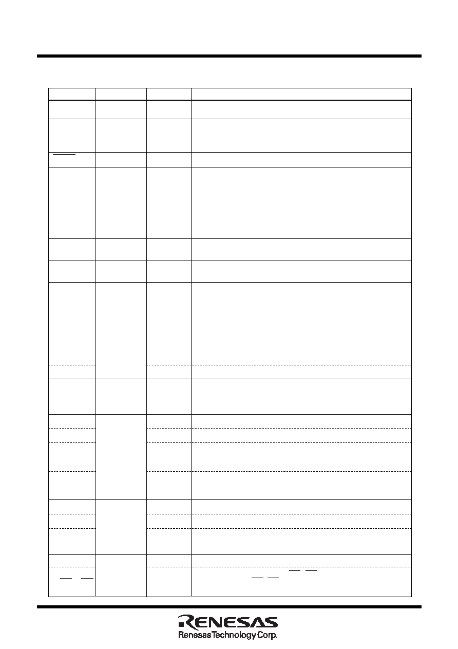
Pin Description
8
Mitsubishi microcomputers
M16C / 62N Group
SINGLE-CHIP 16-BIT CMOS MICROCOMPUTER
VCC, VSS
CNVSS
XIN
XOUT
BYTE
AVCC
AVSS
VREF
P00 to P07
D0 to D7
P10 to P17
D8 to D15
P20 to P27
A0 to A7
A0/D0 to
A7/D7
A0
A1/D0
to A7/D6
P30 to P37
A8 to A15
A8/D7,
A9 to A15
P40 to P47
Signal name
Power supply
input
CNVSS
Reset input
Clock input
Clock output
External data
bus width
select input
Analog power
supply input
Reference
voltage input
I/O port P0
I/O port P1
I/O port P2
I/O port P3
I/O port P4
Supply 2.2V to 3.6 V (mask ROM version), 2.4V to 3.6 V (flash memory
version) to the VCC pin. Supply 0 V to the VSS pin.
Function
This pin switches between processor modes. Connect this pin to the
VSS pin when after a reset you want to start operation in single-chip
mode (memory expansion mode) or the VCC pin when starting
operation in microprocessor mode.
A “L” on this input resets the microcomputer.
These pins are provided for the main clock generating circuit.Connect
a ceramic resonator or crystal between the XIN and the XOUT pins. To
use an externally derived clock, input it to the XIN pin and leave the
XOUT pin open.
This pin selects the width of an external data bus. A 16-bit width is
selected when this input is “L”; an 8-bit width is selected when this
input is “H”. This input must be fixed to either “H” or “L”. Connect this
pin to the VSS pin when not using external data bus.
This pin is a power supply input for the A-D converter. Connect this
pin to VCC.
This pin is a power supply input for the A-D converter. Connect this
pin to VSS.
This pin is a reference voltage input for the A-D converter.
This is an 8-bit CMOS I/O port. It has an input/output port direction
register that allows the user to set each pin for input or output
individually. When used for input in single-chip mode, the port can be
set to have or not have a pull-up resistor in units of four bits by
software. In memory expansion and microprocessor modes, selection
of the internal pull-resistor is not available.
When used for single-chip mode, P0 also function as A-D converter
extended input pins as selected by software.
When set as a separate bus, these pins input and output data (D0–D7).
This is an 8-bit I/O port equivalent to P0. P15 to P17 also function as
external interrupt pins as selected by software.
When set as a separate bus, these pins input and output data (D8–D15).
This is an 8-bit I/O port equivalent to P0.
These pins output 8 low-order address bits (A0–A7).
If the external bus is set as an 8-bit wide multiplexed bus, these pins
input and output data (D0–D7) and output 8 low-order address bits
(A0–A7) separated in time by multiplexing.
If the external bus is set as a 16-bit wide multiplexed bus, these pins
input and output data (D0–D6) and output address (A1–A7) separated
in time by multiplexing. They also output address (A0).
This is an 8-bit I/O port equivalent to P0.
These pins output 8 middle-order address bits (A8–A15).
If the external bus is set as a 16-bit wide multiplexed bus, these pins
input and output data (D7) and output address (A8) separated in time
by multiplexing. They also output address (A9–A15).
This is an 8-bit I/O port equivalent to P0.
Pin name
Input
Output
Input
Input/output
I/O type
Analog power
supply input
Input/output
Output
Input/output
Output
Input/output
Output
Input/output
Output
Input/output
Output
A16 to A19,
CS0 to CS3
These pins output A16–A19 and CS0–CS3 signals. A16–A19 are 4 high-
order address bits. CS0–CS3 are chip select signals used to specify an
access space.
RESET
Pin Description
相关PDF资料 |
PDF描述 |
|---|---|
| M30620SGP | 16-BIT, 16 MHz, MICROCONTROLLER, PQFP100 |
| M30620MA-XXXGP | 16-BIT, MROM, 16 MHz, MICROCONTROLLER, PQFP100 |
| M30620MC-XXXFP | 16-BIT, MROM, 16 MHz, MICROCONTROLLER, PQFP100 |
| M30620SFP | 16-BIT, 16 MHz, MICROCONTROLLER, PQFP100 |
| M30622MA-XXXGP | 16-BIT, MROM, 16 MHz, MICROCONTROLLER, PQFP100 |
相关代理商/技术参数 |
参数描述 |
|---|---|
| M30624MGP | 制造商:RENESAS 制造商全称:Renesas Technology Corp 功能描述:SINGLE-CHIP 16-BIT CMOS MICROCOMPUTER |
| M30624MGP-XXXFP | 制造商:RENESAS 制造商全称:Renesas Technology Corp 功能描述:SINGLE-CHIP 16-BIT CMOS MICROCOMPUTER |
| M30624MGP-XXXGP | 制造商:RENESAS 制造商全称:Renesas Technology Corp 功能描述:SINGLE-CHIP 16-BIT CMOS MICROCOMPUTER |
| M30624MG-XXXFP | 制造商:RENESAS 制造商全称:Renesas Technology Corp 功能描述:16-BIT SINGLE-CHIP MICROCOMPUTER M16C FAMILY |
| M30624MG-XXXGP | 制造商:RENESAS 制造商全称:Renesas Technology Corp 功能描述:16-BIT SINGLE-CHIP MICROCOMPUTER M16C FAMILY |
发布紧急采购,3分钟左右您将得到回复。