- 您现在的位置:买卖IC网 > PDF目录80481 > M3062JFHVGP-B 16-BIT, FLASH, 24 MHz, MICROCONTROLLER, PQFP100 PDF资料下载
参数资料
| 型号: | M3062JFHVGP-B |
| 元件分类: | 微控制器/微处理器 |
| 英文描述: | 16-BIT, FLASH, 24 MHz, MICROCONTROLLER, PQFP100 |
| 封装: | 14 X 14 MM, 0.50 MM PITCH, PLASTIC, LQFP-100 |
| 文件页数: | 13/87页 |
| 文件大小: | 919K |
| 代理商: | M3062JFHVGP-B |
第1页第2页第3页第4页第5页第6页第7页第8页第9页第10页第11页第12页当前第13页第14页第15页第16页第17页第18页第19页第20页第21页第22页第23页第24页第25页第26页第27页第28页第29页第30页第31页第32页第33页第34页第35页第36页第37页第38页第39页第40页第41页第42页第43页第44页第45页第46页第47页第48页第49页第50页第51页第52页第53页第54页第55页第56页第57页第58页第59页第60页第61页第62页第63页第64页第65页第66页第67页第68页第69页第70页第71页第72页第73页第74页第75页第76页第77页第78页第79页第80页第81页第82页第83页第84页第85页第86页第87页
1. Overview
M16C/62P Group (M16C/62P, M16C/62PT)
4
8
f
o
4
0
2
,
1
0
p
e
S
0
3
.
2
.
v
e
R
Z
0
3
2
0
-
1
0
B
3
0
J
E
R
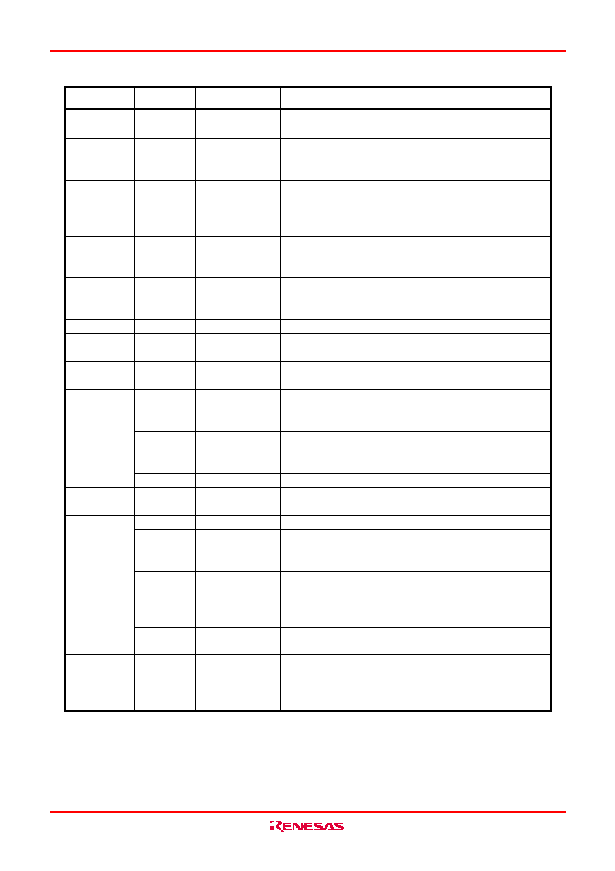
page 20
Apply 2.7 to 5.5 V to the VCC1 pin and 0 V to the VSS pin. (2)
Applies the power supply for the A/D converter. Connect the AVCC pin to
VCC1. Connect the AVSS pin to VSS.
The microcomputer is in a reset state when applying "L" to the this pin.
Switches processor mode. Connect this pin to VSS to when after a reset to
start up in single-chip mode. Connect this pin to VCC1 to start up in micropro-
cessor mode. As for the BYTE pin of the 80-pin versions, pull-up processing
is performed within the microcomputer.
I/O pins for the main clock generation circuit. Connect a ceramic resonator or
crystal oscillator between XIN and XOUT (3). To use the external clock, input
the clock from XIN and leave XOUT open.
I/O pins for a sub clock oscillation circuit. Connect a crystal oscillator between
XCIN and XCOUT (3). To use the external clock, input the clock from XCIN
and leave XCOUT open.
The clock of the same cycle as fC, f8, or f32 is outputted.
______
Input pins for the INT interrupt
_______
Input pin for the NMI interrupt.
Input pins for the key input interrupt
These are timer A0, timer A3 and Timer A4 I/O pins. (except the output of
TAOUT for the N-channel open drain output.)
These are timer A0, timer A3 and Timer A4 input pins.
Input pin for the Z-phase.
These are timer B0, timer B2 to timer B5 input pins.
These are send control input pins.
These are receive control output pins.
These are transfer clock I/O pins.
These are serial data input pins.
These are serial data output pins. (except TXD2 for the N-channel open drain
output.)
These are serial data output pins.
This is output pin for transfer clock output from multiple pins function.
These are serial data I/O pins. (except SDA2 for the N-channel open drain
output.)
These are transfer clock I/O pins. (except SCL2 for the N-channel open drain
output.)
VCC1,
VSS
AVCC,
AVSS
____________
RESET
CNVSS
(BYTE)
XIN
XOUT
XCIN
XCOUT
CLKOUT
________
INT0 to INT2
_______
NMI
______
KI0 to KI3
TA0OUT,
TA3OUT,
TA4OUT
TA0IN,
TA3IN,
TA4IN
ZP
TB0IN,
TB2IN to TB5IN
_________
CTS0, CTS2
_________
RTS0, RTS2
CLK0, CLK1,
CLK3, CLK4
RXD0 to RXD2
SIN4
TXD0 to TXD4
SOUT3, SOUT4
CLKS1
SDA0 to SDA2
SCL0 to SCL2
Power supply input
Analog power
supply input
Reset input
CNVSS
Main clock input
Main clock output
Sub clock input
Sub clock output
Clock output
______
INT interrupt input
_______
NMI interrupt input
Key input interrupt
input
Timer A
Timer B
Serial I/O
I2C mode
I
O
I
O
I
I/O
I
O
I/O
I
O
I/O
-
VCC1
VCC2
VCC1
Power
Signal Name
Pin Name I/O Type
Description
Supply
I : Input
O : Output
I/O : Input and output
NOTES:
1. In this manual, hereafter, VCC refers to VCC1 unless otherwise noted.
2. In M16C/62PT, apply 4.0 to 5.5 V to the VCC1 pin.
3. Ask the oscillator maker the oscillation characteristic.
Table 1.13 Pin Description (80-pin Version) (1)
相关PDF资料 |
PDF描述 |
|---|---|
| MTFDCAE004SAJ-1M1IT | FLOPPY DISK DRIVE CONTROLLER, XMA |
| MC9S08JS16CWJ | MICROCONTROLLER, PDSO20 |
| MC9S12GC64CFU | 16-BIT, FLASH, 25 MHz, MICROCONTROLLER, PQFP80 |
| MC9S12GC96MFA | 16-BIT, FLASH, 25 MHz, MICROCONTROLLER, PQFP48 |
| MN103SA5K | 32-BIT, MROM, MICROCONTROLLER, PQFP100 |
相关代理商/技术参数 |
参数描述 |
|---|---|
| M3062LFGPFP | 制造商:RENESAS 制造商全称:Renesas Technology Corp 功能描述:SINGLE-CHIP 16-BIT CMOS MICROCOMPUTER |
| M3062LFGPFP#U3C | 功能描述:IC M16C/62P MCU FLASH 100-QFP RoHS:是 类别:集成电路 (IC) >> 嵌入式 - 微控制器, 系列:M16C™ M16C/60/62P 标准包装:96 系列:PIC® 16F 核心处理器:PIC 芯体尺寸:8-位 速度:20MHz 连通性:I²C,SPI 外围设备:欠压检测/复位,POR,PWM,WDT 输入/输出数:11 程序存储器容量:3.5KB(2K x 14) 程序存储器类型:闪存 EEPROM 大小:- RAM 容量:128 x 8 电压 - 电源 (Vcc/Vdd):2.3 V ~ 5.5 V 数据转换器:A/D 8x10b 振荡器型:内部 工作温度:-40°C ~ 125°C 封装/外壳:14-TSSOP(0.173",4.40mm 宽) 包装:管件 |
| M3062LFGPFP#U5C | 功能描述:IC M16C/62P MCU FLASH 100-QFP RoHS:是 类别:集成电路 (IC) >> 嵌入式 - 微控制器, 系列:M16C™ M16C/60/62P 标准包装:96 系列:PIC® 16F 核心处理器:PIC 芯体尺寸:8-位 速度:20MHz 连通性:I²C,SPI 外围设备:欠压检测/复位,POR,PWM,WDT 输入/输出数:11 程序存储器容量:3.5KB(2K x 14) 程序存储器类型:闪存 EEPROM 大小:- RAM 容量:128 x 8 电压 - 电源 (Vcc/Vdd):2.3 V ~ 5.5 V 数据转换器:A/D 8x10b 振荡器型:内部 工作温度:-40°C ~ 125°C 封装/外壳:14-TSSOP(0.173",4.40mm 宽) 包装:管件 |
| M3062LFGPFP#U7C | 功能描述:IC M16C/62P MCU FLASH 100-QFP RoHS:是 类别:集成电路 (IC) >> 嵌入式 - 微控制器, 系列:M16C™ M16C/60/62P 产品培训模块:CAN Basics Part-1 CAN Basics Part-2 Electromagnetic Noise Reduction Techniques Part 1 M16C Product Overview Part 1 M16C Product Overview Part 2 标准包装:1 系列:M16C™ M32C/80/87 核心处理器:M32C/80 芯体尺寸:16/32-位 速度:32MHz 连通性:EBI/EMI,I²C,IEBus,IrDA,SIO,UART/USART 外围设备:DMA,POR,PWM,WDT 输入/输出数:121 程序存储器容量:384KB(384K x 8) 程序存储器类型:闪存 EEPROM 大小:- RAM 容量:24K x 8 电压 - 电源 (Vcc/Vdd):3 V ~ 5.5 V 数据转换器:A/D 34x10b,D/A 2x8b 振荡器型:内部 工作温度:-20°C ~ 85°C 封装/外壳:144-LQFP 包装:托盘 产品目录页面:749 (CN2011-ZH PDF) 配用:R0K330879S001BE-ND - KIT DEV RSK M32C/87 |
| M3062LFGPFP#U9C | 功能描述:IC M16C/62P MCU FLASH 100-QFP RoHS:是 类别:集成电路 (IC) >> 嵌入式 - 微控制器, 系列:M16C™ M16C/60/62P 标准包装:1 系列:87C 核心处理器:MCS 51 芯体尺寸:8-位 速度:16MHz 连通性:SIO 外围设备:- 输入/输出数:32 程序存储器容量:8KB(8K x 8) 程序存储器类型:OTP EEPROM 大小:- RAM 容量:256 x 8 电压 - 电源 (Vcc/Vdd):4 V ~ 6 V 数据转换器:- 振荡器型:外部 工作温度:0°C ~ 70°C 封装/外壳:44-DIP 包装:管件 其它名称:864285 |
发布紧急采购,3分钟左右您将得到回复。