- 您现在的位置:买卖IC网 > PDF目录80361 > M306N4FGTFP#U0 16-BIT, FLASH, 20 MHz, MICROCONTROLLER, PQFP100 PDF资料下载
参数资料
| 型号: | M306N4FGTFP#U0 |
| 元件分类: | 微控制器/微处理器 |
| 英文描述: | 16-BIT, FLASH, 20 MHz, MICROCONTROLLER, PQFP100 |
| 封装: | 14 X 20 MM, 0.65 MM PITCH, PLASTIC, QFP-100 |
| 文件页数: | 6/92页 |
| 文件大小: | 694K |
| 代理商: | M306N4FGTFP#U0 |
第1页第2页第3页第4页第5页当前第6页第7页第8页第9页第10页第11页第12页第13页第14页第15页第16页第17页第18页第19页第20页第21页第22页第23页第24页第25页第26页第27页第28页第29页第30页第31页第32页第33页第34页第35页第36页第37页第38页第39页第40页第41页第42页第43页第44页第45页第46页第47页第48页第49页第50页第51页第52页第53页第54页第55页第56页第57页第58页第59页第60页第61页第62页第63页第64页第65页第66页第67页第68页第69页第70页第71页第72页第73页第74页第75页第76页第77页第78页第79页第80页第81页第82页第83页第84页第85页第86页第87页第88页第89页第90页第91页第92页
Rev.2.40
Aug 25, 2006
page 14 of 88
REJ03B0003-0240
M16C/6N Group (M16C/6N4)
3. Memory
Under development
This document is under development and its contents are subject to change.
3. Memory
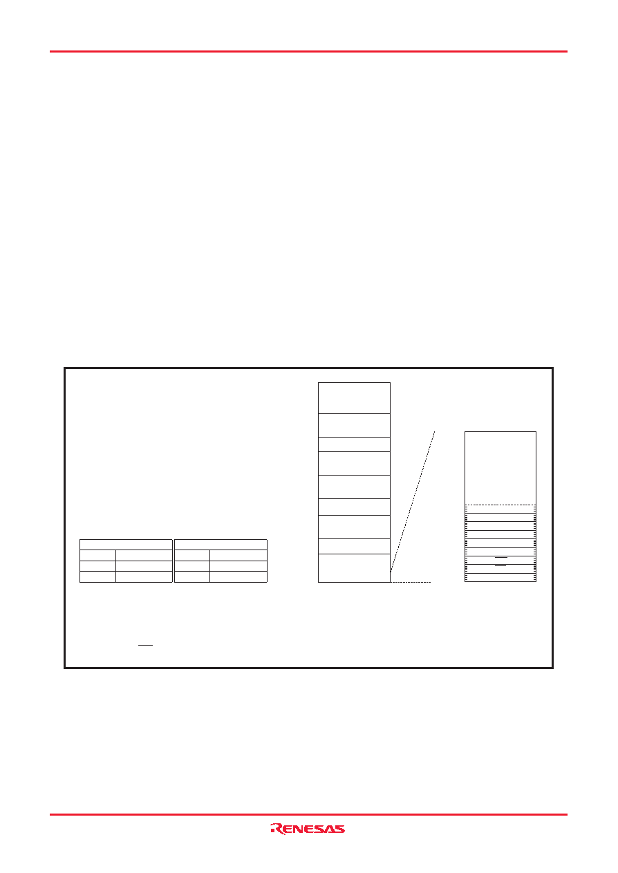
Figure 3.1 shows a Memory Map. The address space extends the 1 Mbyte from address 00000h to FFFFFh.
The internal ROM is allocated in a lower address direction beginning with address FFFFFh. For example, a
128-Kbyte internal ROM is allocated to the addresses from E0000h to FFFFFh.
As for the flash memory version, 4-Kbyte space (block A) exists in 0F000h to 0FFFFh. 4-Kbyte space is
mainly for storing data. In addition to storing data, 4-Kbyte space also can store programs.
The fixed interrupt vector table is allocated to the addresses from FFFDCh to FFFFFh. Therefore, store the
start address of each interrupt routine here.
The internal RAM is allocated in an upper address direction beginning with address 00400h. For example, a
5-Kbyte internal RAM is allocated to the addresses from 00400h to 017FFh. In addition to storing data, the
internal RAM also stores the stack used when calling subroutines and when interrupts are generated.
The Special Function Registers (SFRs) are allocated to the addresses from 00000h to 003FFh. Peripheral
function control registers are located here. Of the SFR, any area which has no functions allocated is reserved
for future use and cannot be accessed by user.
The special page vector table is allocated to the addresses from FFE00h to FFFDBh. This vector is used by
the JMPS or JSRS instruction. For details, refer to M16C/60, M16C/20, M16C/Tiny Series Software Manual.
In memory expansion and microprocessor modes, some areas are reserved for future use and cannot be
used by users.
Figure 3.1 Memory Map
00000h
YYYYYh
FFFFFh
00400h
0FFFFh
10000h
0F000h
27000h
28000h
80000h
XXXXXh
Internal ROM
(data flash) (3)
Internal ROM
(program area) (4)
SFR
Internal RAM
Reserved area
External area
Reserved area (2)
External area
FFE00h
FFFDCh
FFFFFh
NOTES:
1. During memory expansion mode or microprocessor mode, cannot be used.
2. In memory expansion mode, cannot be used.
3. As for the flash memory version, 4-Kbyte space (block A) exists.
4. When using the masked ROM version, write nothing to internal ROM area.
5. Shown here is a memory map for the case where the PM10 bit in the PM1 register is 1 (block A enabled, addresses 10000h to
26FFFh for CS2 area) and the PM13 bit in the PM1 register is 1 (internal RAM area is expanded over 192 Kbytes).
Undefined instruction
Overflow
BRK instruction
Address match
Single step
Oscillation stop and re-oscillation
detection / watchdog timer
Reset
Special page
vector table
DBC
NMI
Address XXXXXh
Capacity
Internal RAM
10 Kbytes
02BFFh
5 Kbytes
017FFh
Address YYYYYh
Capacity
Internal ROM (4)
256 Kbytes
C0000h
128 Kbytes
E0000h
Reserved area (1)
相关PDF资料 |
PDF描述 |
|---|---|
| M306N4MCT-XXXGP | 16-BIT, MROM, 20 MHz, MICROCONTROLLER, PQFP100 |
| M306NNME-XXXGP | 16-BIT, MROM, 24 MHz, MICROCONTROLLER, PQFP128 |
| M30882FHTGP | 32-BIT, FLASH, 32 MHz, MICROCONTROLLER, PQFP144 |
| M32176F4VFP | 32-BIT, FLASH, 32 MHz, RISC MICROCONTROLLER, PQFP144 |
| M37547G4FP | 8-BIT, MROM, 8 MHz, MICROCONTROLLER, PDSO36 |
相关代理商/技术参数 |
参数描述 |
|---|---|
| M306N4FGTGP | 制造商:Renesas Electronics Corporation 功能描述: |
| M306N4FGVFP | 功能描述:IC M16C MCU FLASH 100QFP RoHS:否 类别:集成电路 (IC) >> 嵌入式 - 微控制器, 系列:M16C™ M16C/60/6N4 标准包装:60 系列:PSOC® 3 CY8C38xx 核心处理器:8051 芯体尺寸:8-位 速度:67MHz 连通性:EBI/EMI,I²C,LIN,SPI,UART/USART 外围设备:电容感应,DMA,LCD,POR,PWM,WDT 输入/输出数:25 程序存储器容量:64KB(64K x 8) 程序存储器类型:闪存 EEPROM 大小:2K x 8 RAM 容量:8K x 8 电压 - 电源 (Vcc/Vdd):1.71 V ~ 5.5 V 数据转换器:A/D 2x20b,D/A 4x8b 振荡器型:内部 工作温度:-40°C ~ 85°C 封装/外壳:48-VFQFN 裸露焊盘 包装:托盘 |
| M306N4FGVFP#UKJ | 制造商:Renesas Electronics Corporation 功能描述:16-BIT M16C CISC - Bulk |
| M306N4FGVGP | 制造商:Renesas Electronics Corporation 功能描述: |
| M306N4FGVGP#U0 | 制造商:Renesas Electronics Corporation 功能描述: |
发布紧急采购,3分钟左右您将得到回复。