- 您现在的位置:买卖IC网 > PDF目录80445 > M306N5MCT-XXXGP 16-BIT, MROM, 20 MHz, MICROCONTROLLER, PQFP100 PDF资料下载
参数资料
| 型号: | M306N5MCT-XXXGP |
| 元件分类: | 微控制器/微处理器 |
| 英文描述: | 16-BIT, MROM, 20 MHz, MICROCONTROLLER, PQFP100 |
| 封装: | 14 X 14 MM, 0.50 MM PITCH, PLASTIC, LQFP-100 |
| 文件页数: | 2/88页 |
| 文件大小: | 683K |
| 代理商: | M306N5MCT-XXXGP |
第1页当前第2页第3页第4页第5页第6页第7页第8页第9页第10页第11页第12页第13页第14页第15页第16页第17页第18页第19页第20页第21页第22页第23页第24页第25页第26页第27页第28页第29页第30页第31页第32页第33页第34页第35页第36页第37页第38页第39页第40页第41页第42页第43页第44页第45页第46页第47页第48页第49页第50页第51页第52页第53页第54页第55页第56页第57页第58页第59页第60页第61页第62页第63页第64页第65页第66页第67页第68页第69页第70页第71页第72页第73页第74页第75页第76页第77页第78页第79页第80页第81页第82页第83页第84页第85页第86页第87页第88页
Rev.2.40
Aug 25, 2006
page 10 of 84
REJ03B0004-0240
M16C/6N Group (M16C/6N5)
1. Overview
Under development
This document is under development and its contents are subject to change.
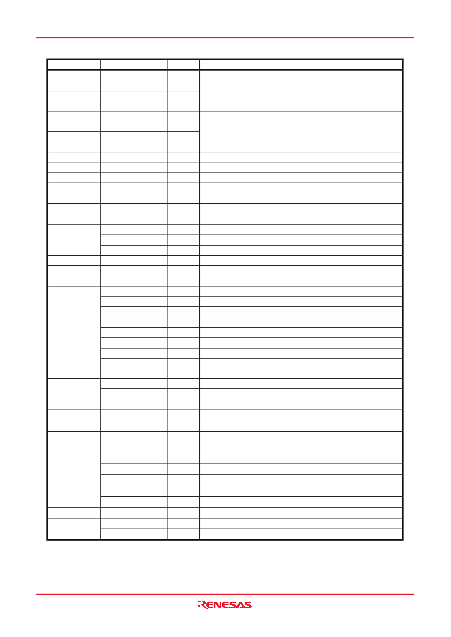
Table 1.6 Pin Functions (2)
I
O
I
O
I
I/O
I
O
I
O
I/O
I
O
I/O
I
I/O
I
O
I
O
XIN
XOUT
XCIN
XCOUT
BCLK
CLKOUT
________
INT0 to INT5
________
NMI
______
KI0 to KI3
TA0OUT to TA4OUT
TA0IN to TA4IN
ZP
TB0IN to TB5IN
___
____
U, U, V, V, W, W
__________
CTS0 to CTS2
__________
RTS0 to RTS2
CLK0 to CLK3
RXD0 to RXD2
SIN3
TXD0 to TXD2
SOUT3
CLKS1
SDA0 to SDA2
SCL0 to SCL2
VREF
AN0 to AN7
AN0_0 to AN0_7
AN2_0 to AN2_7
_____________
ADTRG
ANEX0
ANEX1
DA0, DA1
CRX0
CTX0
Main clock
input
Main clock
output
Sub clock
input
Sub clock
output
BCLK output
Clock output
INT interrupt input
_______
NMI interrupt
input
Key input
interrupt input
Timer A
Timer B
Three-phase motor
control output
Serial interface
I
2C mode
Reference
voltage input
A/D converter
D/A converter
CAN module
I/O pins for the main clock oscillation circuit. Connect a ceramic
resonator or crystal oscillator between XIN and XOUT
(1).
To use the external clock, input the clock from XIN and leave
XOUT open.
I/O pins for a sub clock oscillation circuit. Connect a crystal
oscillator between XCIN and XCOUT
(1).
To use the external clock, input the clock from XCIN and leave
XCOUT open.
Outputs the BCLK signal.
The clock of the same cycle as fC, f8, or f32 is output.
______
Input pins for the INT interrupt.
_______
Input pin for the NMI interrupt.
Input pins for the key input interrupt.
These are timer A0 to timer A4 I/O pins.
These are timer A0 to timer A4 input pins.
Input pin for the Z-phase.
These are timer B0 to timer B5 input pins.
These are Three-phase motor control output pins.
These are transmit control input pins.
These are receive control output pins.
These are transfer clock I/O pins.
These are serial data input pins.
These are serial data output pins.
This is output pin for transfer clock output from multiple pins
function.
These are serial data I/O pins.
These are transfer clock I/O pins. (however, SCL2 for the
N-channel open drain output.)
Applies the reference voltage for the A/D converter and D/A
converter.
Analog input pins for the A/D converter.
This is an A/D trigger input pin.
This is the extended analog input pin for the A/D converter,
and is the output in external op-amp connection mode.
This is the extended analog input pin for the A/D converter.
These are the output pins for the D/A converter.
This is the input pin for the CAN module.
This is the output pin for the CAN module.
Signal Name
Pin Name
I/O Type
Description
I: Input
O: Output
I/O: Input/Output
NOTE:
1. Ask the oscillator maker the oscillation characteristic.
相关PDF资料 |
PDF描述 |
|---|---|
| MC908GZ16VFA | 8-BIT, FLASH, 8 MHz, MICROCONTROLLER, PQFP48 |
| MC908QY4MDT | 8-BIT, FLASH, 8 MHz, MICROCONTROLLER, PDSO16 |
| MC9S08SH4MTJ | MICROCONTROLLER, PDSO20 |
| MC9S12P32J0VQKR | MICROCONTROLLER, PQFP80 |
| MC9S12P96J0CLH | MICROCONTROLLER, PQFP64 |
相关代理商/技术参数 |
参数描述 |
|---|---|
| M306N5MCV-XXXFP | 制造商:RENESAS 制造商全称:Renesas Technology Corp 功能描述:Renesas MCU |
| M306N5MCV-XXXGP | 制造商:RENESAS 制造商全称:Renesas Technology Corp 功能描述:Renesas MCU |
| M306N5MC-XXXGP | 制造商:RENESAS 制造商全称:Renesas Technology Corp 功能描述:Renesas MCU |
| M306NKFHGP | 制造商:RENESAS 制造商全称:Renesas Technology Corp 功能描述:Renesas MCU |
| M306NKFHGP#U3 | 功能描述:IC M16C MCU FLASH 384K 100LQFP RoHS:是 类别:集成电路 (IC) >> 嵌入式 - 微控制器, 系列:M16C™ M16C/60/6NK 标准包装:1 系列:AVR® ATmega 核心处理器:AVR 芯体尺寸:8-位 速度:16MHz 连通性:I²C,SPI,UART/USART 外围设备:欠压检测/复位,POR,PWM,WDT 输入/输出数:32 程序存储器容量:32KB(16K x 16) 程序存储器类型:闪存 EEPROM 大小:1K x 8 RAM 容量:2K x 8 电压 - 电源 (Vcc/Vdd):2.7 V ~ 5.5 V 数据转换器:A/D 8x10b 振荡器型:内部 工作温度:-40°C ~ 125°C 封装/外壳:44-TQFP 包装:剪切带 (CT) 其它名称:ATMEGA324P-B15AZCT |
发布紧急采购,3分钟左右您将得到回复。