- 您现在的位置:买卖IC网 > PDF目录67760 > M306NKFJTGP 16-BIT, FLASH, 20 MHz, MICROCONTROLLER, PQFP100 PDF资料下载
参数资料
| 型号: | M306NKFJTGP |
| 元件分类: | 微控制器/微处理器 |
| 英文描述: | 16-BIT, FLASH, 20 MHz, MICROCONTROLLER, PQFP100 |
| 封装: | 14 X 14 MM, 0.50 MM PITCH, PLASTIC, LQFP-100 |
| 文件页数: | 6/84页 |
| 文件大小: | 586K |
| 代理商: | M306NKFJTGP |
第1页第2页第3页第4页第5页当前第6页第7页第8页第9页第10页第11页第12页第13页第14页第15页第16页第17页第18页第19页第20页第21页第22页第23页第24页第25页第26页第27页第28页第29页第30页第31页第32页第33页第34页第35页第36页第37页第38页第39页第40页第41页第42页第43页第44页第45页第46页第47页第48页第49页第50页第51页第52页第53页第54页第55页第56页第57页第58页第59页第60页第61页第62页第63页第64页第65页第66页第67页第68页第69页第70页第71页第72页第73页第74页第75页第76页第77页第78页第79页第80页第81页第82页第83页第84页
Rev.2.10
Aug 25, 2006
page 14 of 81
REJ03B0058-02100
M16C/6N Group (M16C/6NK, M16C/6NM)
1. Overview
Under development
This document is under development and its contents are subject to change.
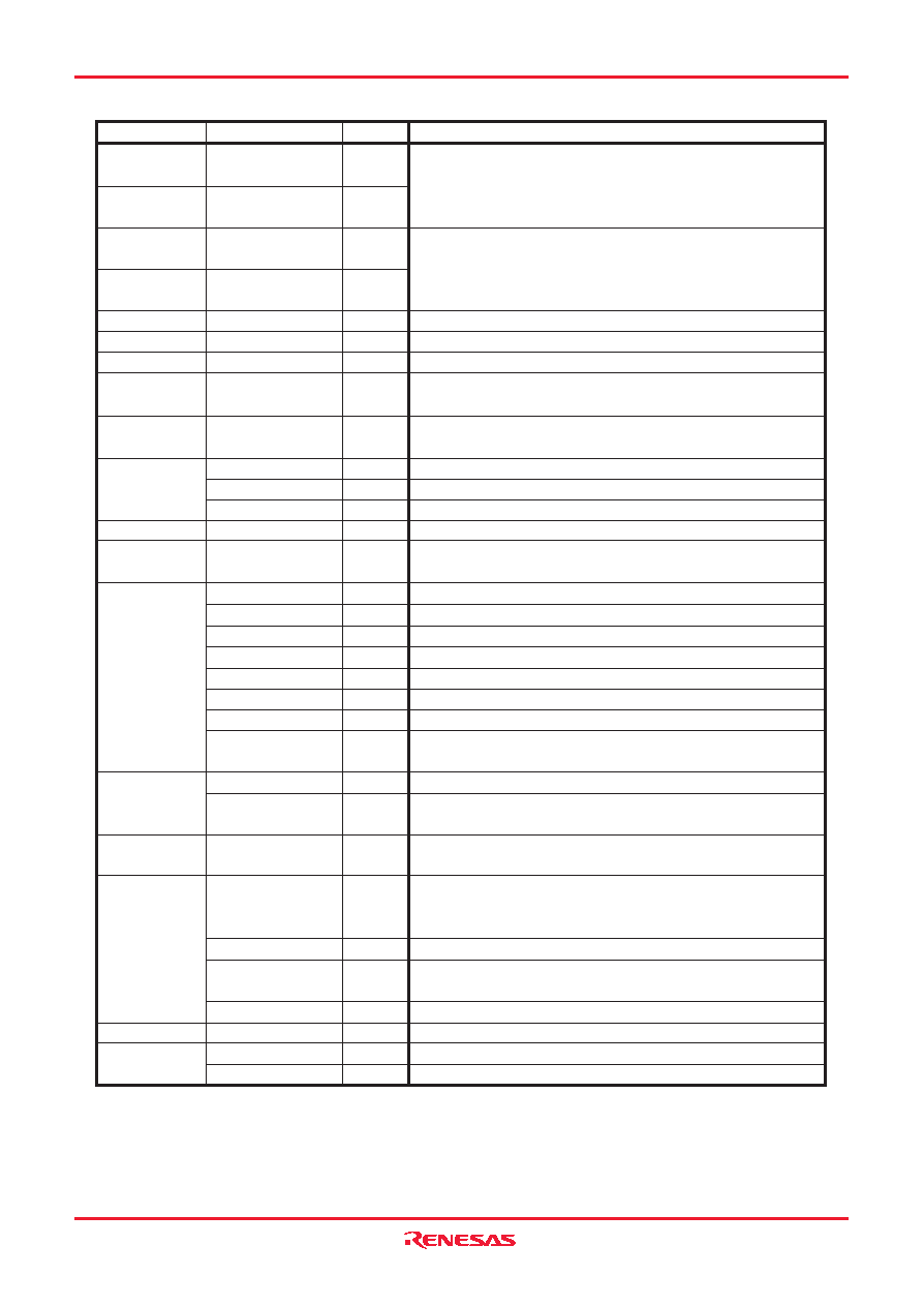
Table 1.10 Pin Functions (100-pin and 128-pin Versions) (2)
I
O
I
O
I
I/O
I
O
I
O
I/O
I
O
I/O
I
I/O
I
O
I
O
XIN
XOUT
XCIN
XCOUT
BCLK
CLKOUT
NT0 to INT8
(2)
________
NMI
______
KI0 to KI3
TA0OUT to TA4OUT
TA0IN to TA4IN
ZP
TB0IN to TB5IN
___
____
U, U, V, V, W, W
__________
CTS0 to CTS2
__________
RTS0 to RTS2
CLK0 to CLK6
(2)
RXD0 to RXD2
SIN3 to SIN6
(2)
TXD0 to TXD2
SOUT3 to SOUT6
(2)
CLKS1
SDA0 to SDA2
SCL0 to SCL2
VREF
AN0 to AN7
AN0_0 to AN0_7
AN2_0 to AN2_7
_____________
ADTRG
ANEX0
ANEX1
DA0, DA1
CRX0, CRX1
CTX0, CTX1
Main clock
input
Main clock
output
Sub clock
input
Sub clock
output
BCLK output
(3)
Clock output
INT interrupt input
_______
NMI interrupt
input
Key input
interrupt input
Timer A
Timer B
Three-phase motor
control output
Serial interface
I
2C mode
Reference
voltage input
A/D converter
D/A converter
CAN module
I/O pins for the main clock oscillation circuit. Connect a ceramic
resonator or crystal oscillator between XIN and XOUT
(1).
To use the external clock, input the clock from XIN and leave
XOUT open.
I/O pins for a sub clock oscillation circuit. Connect a crystal
oscillator between XCIN and XCOUT
(1).
To use the external clock, input the clock from XCIN and leave
XCOUT open.
Outputs the BCLK signal.
The clock of the same cycle as fC, f8, or f32 is output.
______
Input pins for the INT interrupt.
_______
Input pin for the NMI interrupt.
Input pins for the key input interrupt.
These are timer A0 to timer A4 I/O pins.
These are timer A0 to timer A4 input pins.
Input pin for the Z-phase.
These are timer B0 to timer B5 input pins.
These are Three-phase motor control output pins.
These are transmit control input pins.
These are receive control output pins.
These are transfer clock I/O pins.
These are serial data input pins.
These are serial data output pins.
This is output pin for transfer clock output from multiple pins
function.
These are serial data I/O pins.
These are transfer clock I/O pins. (however, SCL2 for
the N-channel open drain output.)
Applies the reference voltage for the A/D converter and D/A
converter.
Analog input pins for the A/D converter.
This is an A/D trigger input pin.
This is the extended analog input pin for the A/D converter,
and is the output in external op-amp connection mode.
This is the extended analog input pin for the A/D converter.
These are the output pins for the D/A converter.
These are the input pins for the CAN module.
These are the output pins for the CAN module.
Signal Name
Pin Name
I/O Type
Description
I: Input
O: Output
I/O: Input/Output
NOTES:
1. Ask the oscillator maker the oscillation characteristic.
________
2. INT6 to INT8, CLK5, CLK6, SIN5, SIN6, SOUT5, SOUT6 are only in the 128-pin version.
3. Not available the bus control pins in T/V-ver..
相关PDF资料 |
PDF描述 |
|---|---|
| M306NKMG-XXXGP | 16-BIT, MROM, 24 MHz, MICROCONTROLLER, PQFP100 |
| M306NMFHGP | 16-BIT, FLASH, 24 MHz, MICROCONTROLLER, PQFP128 |
| M306NKFHTGP | 16-BIT, FLASH, 20 MHz, MICROCONTROLLER, PQFP100 |
| M306NKFJGP | 16-BIT, FLASH, 24 MHz, MICROCONTROLLER, PQFP100 |
| M306NMFJGP | 16-BIT, FLASH, 24 MHz, MICROCONTROLLER, PQFP128 |
相关代理商/技术参数 |
参数描述 |
|---|---|
| M306NKFJVGP | 制造商:RENESAS 制造商全称:Renesas Technology Corp 功能描述:Renesas MCU |
| M306NKFJVGP#U0 | 制造商:Renesas Electronics Corporation 功能描述: |
| M306NKME-XXXGP | 制造商:RENESAS 制造商全称:Renesas Technology Corp 功能描述:Renesas MCU |
| M306NKMG-XXXGP | 制造商:RENESAS 制造商全称:Renesas Technology Corp 功能描述:Renesas MCU |
| M306NKT-EPB | 功能描述:EMULATOR PROBE M16C/6N RoHS:否 类别:编程器,开发系统 >> 配件 系列:- 产品培训模块:Lead (SnPb) Finish for COTS Obsolescence Mitigation Program RoHS指令信息:IButton RoHS Compliance Plan 标准包装:1 系列:- 附件类型:USB 至 1-Wire? RJ11 适配器 适用于相关产品:1-Wire? 设备 产品目录页面:1429 (CN2011-ZH PDF) |
发布紧急采购,3分钟左右您将得到回复。