- 您现在的位置:买卖IC网 > PDF目录102741 > M306V0ME-XXXFP 16-BIT, MROM, 10 MHz, MICROCONTROLLER, PQFP100 PDF资料下载
参数资料
| 型号: | M306V0ME-XXXFP |
| 元件分类: | 微控制器/微处理器 |
| 英文描述: | 16-BIT, MROM, 10 MHz, MICROCONTROLLER, PQFP100 |
| 封装: | 14 X 20 MM, 0.65 MM PITCH, PLASTIC, QFP-100 |
| 文件页数: | 230/251页 |
| 文件大小: | 2165K |
| 代理商: | M306V0ME-XXXFP |
第1页第2页第3页第4页第5页第6页第7页第8页第9页第10页第11页第12页第13页第14页第15页第16页第17页第18页第19页第20页第21页第22页第23页第24页第25页第26页第27页第28页第29页第30页第31页第32页第33页第34页第35页第36页第37页第38页第39页第40页第41页第42页第43页第44页第45页第46页第47页第48页第49页第50页第51页第52页第53页第54页第55页第56页第57页第58页第59页第60页第61页第62页第63页第64页第65页第66页第67页第68页第69页第70页第71页第72页第73页第74页第75页第76页第77页第78页第79页第80页第81页第82页第83页第84页第85页第86页第87页第88页第89页第90页第91页第92页第93页第94页第95页第96页第97页第98页第99页第100页第101页第102页第103页第104页第105页第106页第107页第108页第109页第110页第111页第112页第113页第114页第115页第116页第117页第118页第119页第120页第121页第122页第123页第124页第125页第126页第127页第128页第129页第130页第131页第132页第133页第134页第135页第136页第137页第138页第139页第140页第141页第142页第143页第144页第145页第146页第147页第148页第149页第150页第151页第152页第153页第154页第155页第156页第157页第158页第159页第160页第161页第162页第163页第164页第165页第166页第167页第168页第169页第170页第171页第172页第173页第174页第175页第176页第177页第178页第179页第180页第181页第182页第183页第184页第185页第186页第187页第188页第189页第190页第191页第192页第193页第194页第195页第196页第197页第198页第199页第200页第201页第202页第203页第204页第205页第206页第207页第208页第209页第210页第211页第212页第213页第214页第215页第216页第217页第218页第219页第220页第221页第222页第223页第224页第225页第226页第227页第228页第229页当前第230页第231页第232页第233页第234页第235页第236页第237页第238页第239页第240页第241页第242页第243页第244页第245页第246页第247页第248页第249页第250页第251页
Rev.1.30
Oct 06, 2004
page 8 of 249
M306V0ME-XXXFP, M306V0EEFP
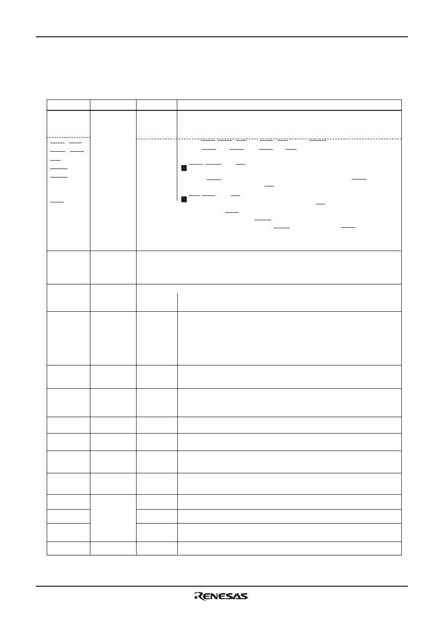
Table 1.5.4 Pin description (continued) (2)
Signal name
Function
Pin name
I/O type
I/O port P5
Input/output
I/O port P6
I/O port P7
P50 to P57
P60 to P63,
P67
P70 to P77
This is an 8-bit I/O port equivalent to P0. In single-chip mode, P57 in
this port outputs a divide-by-8 or divide-by-32 clock of XIN or a clock of
the same frequency as XCIN as selected by software.
Output
Input
Output
Input
This is an 5-bit I/O port equivalent to P0. When set for input in single-chip,
microprocessor and memory expansion modes, the user can specify in units of
four bits via software whether or not they are tied to a pull-up resistor. Pins in
this port also function as UART0 and UART2 pins as selected by software.
This is an 8-bit I/O port equivalent to P6 (P70 and P71 are N-channel
open-drain output). Pins in this port also function as timers A2 and A3,
UART2, or HSYNC counter I/O pins as selected by software.
WRL / WR,
WRH / BHE,
RD,
BCLK,
HLDA,
HOLD,
ALE,
RDY
signals. WRL and WRH, and BHE and WR can be switched using
software control.
WRL, WRH, and RD selected
With a 16-bit external data bus, data is written to even addresses
when the WRL signal is “L” and to the odd addresses when the WRH
signal is “L”. Data is read when RD is “L”.
WR, BHE, and RD selected
Data is written when WR is “L”. Data is read when RD is “L”. Odd addresses are
accessed when BHE is “L”. Use this mode when using an 8-bit external data bus.
While the input level at the HOLD pin is “L”, the microcomputer is placed in the
hold state. While in the hold state, HLDA outputs a “L” level. ALE is used to latch
the address. While the input level of the RDY pin is “L”, the microcomputer is in
Output WRL, WRH (WR and BHE), RD, BCLK, HLDA, and ALE
Input/output
I/O port P8
I/O port P9
I/O port P10
P82, P83,
P86, P87
P90 to P94
P100 to P107
This is an 5-bit I/O port equivalent to P6. Pins in this port also function
as Timer B0 to B2 input pins, or D-A converter output pins.
This is an 8-bit I/O port equivalent to P6. Pins in this port also function
as A-D converter input pins. Furthermore, P100 and P101 also function
as input pins for OSD function.
P82, P83, P86 and P87 are I/O ports with the same functions as P6.
Using software, P82 and P83 can be made to function as the I/O pins for
the input pins for external interrupts. P8 6 and P87 can be set using
software to function as the I/O pins for a sub clock generation circuit. In
this case,connect a quartz oscillator between P86 (XCOUT pin) and P87
(XCIN pin).
R, G, B
OSC1
OSC2
CVIN
VHOLD
HLF
TVSETB
OSD output
Clock input
for OSD
Clock output
for OSD
I/O for data
slicer
Test input
Output
Input
Output
Input
These are OSD output pins (analog output).
This is an OSD clock input pin.
This is an OSD clock output pin.
Input composite video signal through a capacitor.
Connect a capacitor between VHOLD and Vss.
Connect a filter using of a capacitor and a resistor
between HLF and Vss.
This is a test input pin. Fix it to “L.”
OUT1, OUT2
These are OSD output pins (digital output).
OSD output
Output
Input/output
the ready state.
相关PDF资料 |
PDF描述 |
|---|---|
| M32170F6VFP | 32-BIT, FLASH, 40 MHz, RISC MICROCONTROLLER, PQFP240 |
| MB95108AJPFV | 8-BIT, MROM, 16.25 MHz, MICROCONTROLLER, PQFP64 |
| MB90F952JBPFV | 16-BIT, FLASH, 32 MHz, MICROCONTROLLER, PQFP100 |
| MB96F356YWBPMC1-GSE2 | 16-BIT, FLASH, 56 MHz, RISC MICROCONTROLLER, PQFP64 |
| MB91267NAPMC | 32-BIT, MROM, 33 MHz, RISC MICROCONTROLLER, PQFP64 |
相关代理商/技术参数 |
参数描述 |
|---|---|
| M306V2 | 制造商:MITSUBISHI 制造商全称:Mitsubishi Electric Semiconductor 功能描述:SINGLE-CHIP 16-BIT CMOS MICROCOMPUTER with CLOSED CAPTION DECODER and ON-SCREEN DISPLAY CONTROLLER |
| M306V2EEFP | 制造商:MITSUBISHI 制造商全称:Mitsubishi Electric Semiconductor 功能描述:SINGLE-CHIP 16-BIT CMOS MICROCOMPUTER with CLOSED CAPTION DECODER and ON-SCREEN DISPLAY CONTROLLER |
| M306V2EEFS | 功能描述:EPROM MCU/M16C(TV/VTR) EMULATION RoHS:否 类别:编程器,开发系统 >> 配件 系列:- 标准包装:1 系列:- 附件类型:适配器板 适用于相关产品:RCB230,RCB231,RCB212 配用:26790D-ND - RCB BREAKOUT BOARD RS232 CABLE |
| M306V2ME | 制造商:MITSUBISHI 制造商全称:Mitsubishi Electric Semiconductor 功能描述:SINGLE-CHIP 16-BIT CMOS MICROCOMPUTER with CLOSED CAPTION DECODER and ON-SCREEN DISPLAY CONTROLLER |
| M306V2ME-151FP | 制造商:MITSUBISHI 制造商全称:Mitsubishi Electric Semiconductor 功能描述:SINGLE-CHIP 16-BIT CMOS MICROCOMPUTER with CLOSED CAPTION DECODER and ON-SCREEN DISPLAY CONTROLLER |
发布紧急采购,3分钟左右您将得到回复。