- 您现在的位置:买卖IC网 > PDF目录80579 > M30853FHTGP 32-BIT, FLASH, 32 MHz, MICROCONTROLLER, PQFP100 PDF资料下载
参数资料
| 型号: | M30853FHTGP |
| 元件分类: | 微控制器/微处理器 |
| 英文描述: | 32-BIT, FLASH, 32 MHz, MICROCONTROLLER, PQFP100 |
| 封装: | 14 X 14 MM, 0.50 MM PITCH, PLASTIC, LQFP-100 |
| 文件页数: | 10/94页 |
| 文件大小: | 923K |
| 代理商: | M30853FHTGP |
第1页第2页第3页第4页第5页第6页第7页第8页第9页当前第10页第11页第12页第13页第14页第15页第16页第17页第18页第19页第20页第21页第22页第23页第24页第25页第26页第27页第28页第29页第30页第31页第32页第33页第34页第35页第36页第37页第38页第39页第40页第41页第42页第43页第44页第45页第46页第47页第48页第49页第50页第51页第52页第53页第54页第55页第56页第57页第58页第59页第60页第61页第62页第63页第64页第65页第66页第67页第68页第69页第70页第71页第72页第73页第74页第75页第76页第77页第78页第79页第80页第81页第82页第83页第84页第85页第86页第87页第88页第89页第90页第91页第92页第93页第94页
Page 16
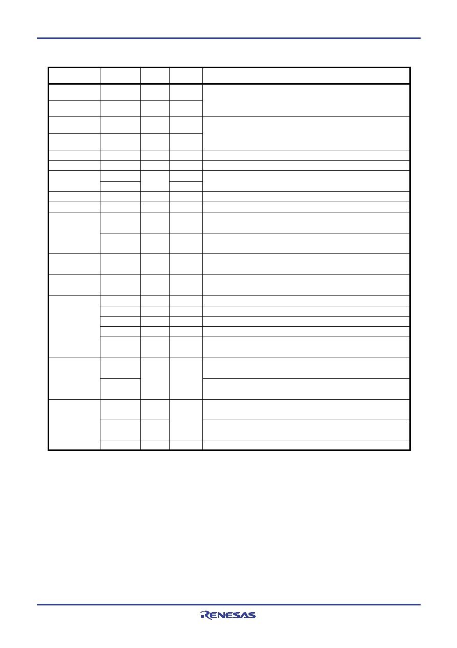
1. Overview
7
8
f
o
5
0
2
,
1
0
.
l
u
J
1
2
.
1
.
v
e
R
)
T
5
8
/
C
2
3
M
,
5
8
/
C
2
3
M
(
p
u
o
r
G
5
8
/
C
2
3
M
XIN
XOUT
XCIN
XCOUT
BCLK
CLKOUT
________
INT0 to INT2
________
INT3 to INT5
_______
NMI
_____
KI0 to KI3
TA0OUT to
TA4OUT
TA0IN to
TA4IN
TB0IN to
TB5IN
___
U, U, V, V,
___
W, W
_________
________
CTS0 to CTS4
_________
RTS0 to RTS4
CLK0 to CLK4
RxD0 to RxD4
TxD0 to TxD4
SDA0 to
SDA4
SCL0 to
SCL4
STxD0 to
STxD4
SRxD0 to
SRxD4
_______
SS0 to SS4
Main Clock Input
Main Clock Output
Sub Clock Input
Sub Clock Output
BCLK Output(1)
Clock Output
______
INT Interrupt
Input
_______
NMI Interrupt Input
Key Input Interrupt
Timer A
Timer B
Three-phase Motor
Control Timer Output
Serial I/O
I2C Mode
Serial I/O
Special Function
VCC1
VCC2
VCC1
VCC2
VCC1
I
O
I
O
I
I/O
I
O
I
O
I/O
I
O
I/O
O
I
I/O pins for the main clock oscillation circuit. Connect a ceramic
resonator or crystal oscillator between XIN and XOUT. To apply
external clock, apply it to XIN and leave XOUT open
I/O pins for the sub clock oscillation circuit. Connect a crystal
oscillator between XCIN and XCOUT. To apply external clock,
apply it to XCIN and leave XCOUT open
Outputs BCLK signal
Outputs the clock having the same frequency as fC, f8 or f32
______
Input pins for the INT interrupt
_______
Input pin for the NMI interrupt
Input pins for the key input interrupt
I/O pins for the timer A0 to A4
(TA0OUT is a pin for the N-channel open drain output.)
Input pins for the timer A0 to A4
Input pins for the timer B0 to B5
Output pins for the three-phase motor control timer
Input pins for data transmission control
Output pins for data reception control
Inputs and outputs the transfer clock
Inputs serial data
Outputs serial data
(TxD2 is a pin for the N-channel open drain output.)
Inputs and outputs serial data
(SDA2 is a pin for the N-channel open drain output.)
Inputs and outputs the transfer clock
(SCL2 is a pin for the N-channel open drain output.)
Outputs serial data when slave mode is selected
(STxD2 is a pin for the N-channel open drain output.)
Inputs serial data when slave mode is selected
Input pins to control serial I/O special function
Supply
Classsfication
Symbol
I/O Type
Function
Voltage
I : Input
O : Output
I/O : Input and output
NOTES:
1. Bus control pins in M32C/85T cannot be used.
Table 1.6 Pin Description (100-Pin and 144-Pin Packages) (Continued)
相关PDF资料 |
PDF描述 |
|---|---|
| M34553M4H-XXXFP | 4-BIT, MROM, 6 MHz, MICROCONTROLLER, PQFP48 |
| M37542M2-XXXHP | 8-BIT, MROM, 8 MHz, MICROCONTROLLER, PQCC36 |
| M38D29GFHP | 8-BIT, FLASH, 6.25 MHz, MICROCONTROLLER, PQFP64 |
| M30201M4-XXXFP | 16-BIT, MROM, 10 MHz, MICROCONTROLLER, PQFP56 |
| M30802SGP-BL | 16-BIT, MROM, 20 MHz, MICROCONTROLLER, PQFP144 |
相关代理商/技术参数 |
参数描述 |
|---|---|
| M30853FJFP | 制造商:RENESAS 制造商全称:Renesas Technology Corp 功能描述:SINGLE-CHIP 16/32-BIT CMOS MICROCOMPUTER |
| M30853FJFP#D3 | 制造商:Renesas Electronics Corporation 功能描述:MCU 16-bit R8C CISC 512KB Flash 5V 100-Pin PQFP 制造商:Renesas Electronics Corporation 功能描述:MCU 16BIT R8C CISC 512KB FLASH 5V 100PQFP - Trays |
| M30853FJFP#D5 | 制造商:Renesas Electronics Corporation 功能描述:MCU 16-Bit R8C CISC 512KB Flash 5V 100-Pin PQFP 制造商:Renesas Electronics Corporation 功能描述:MCU 16BIT R8C CISC 512KB FLASH 5V 100PQFP - Trays |
| M30853FJFP#U3 | 功能描述:IC M32C MCU FLASH 512K 100QFP RoHS:是 类别:集成电路 (IC) >> 嵌入式 - 微控制器, 系列:M16C™ M32C/80/85 标准包装:160 系列:S08 核心处理器:S08 芯体尺寸:8-位 速度:40MHz 连通性:I²C,LIN,SCI,SPI 外围设备:LCD,LVD,POR,PWM,WDT 输入/输出数:53 程序存储器容量:32KB(32K x 8) 程序存储器类型:闪存 EEPROM 大小:- RAM 容量:1.9K x 8 电压 - 电源 (Vcc/Vdd):2.7 V ~ 5.5 V 数据转换器:A/D 12x12b 振荡器型:内部 工作温度:-40°C ~ 105°C 封装/外壳:64-LQFP 包装:托盘 |
| M30853FJFP#U5 | 功能描述:IC M32C MCU FLASH 512K 100QFP RoHS:是 类别:集成电路 (IC) >> 嵌入式 - 微控制器, 系列:M16C™ M32C/80/85 标准包装:160 系列:S08 核心处理器:S08 芯体尺寸:8-位 速度:40MHz 连通性:I²C,LIN,SCI,SPI 外围设备:LCD,LVD,POR,PWM,WDT 输入/输出数:53 程序存储器容量:32KB(32K x 8) 程序存储器类型:闪存 EEPROM 大小:- RAM 容量:1.9K x 8 电压 - 电源 (Vcc/Vdd):2.7 V ~ 5.5 V 数据转换器:A/D 12x12b 振荡器型:内部 工作温度:-40°C ~ 105°C 封装/外壳:64-LQFP 包装:托盘 |
发布紧急采购,3分钟左右您将得到回复。