- 您现在的位置:买卖IC网 > PDF目录80478 > M30855FHTGP 32-BIT, FLASH, 32 MHz, MICROCONTROLLER, PQFP144 PDF资料下载
参数资料
| 型号: | M30855FHTGP |
| 元件分类: | 微控制器/微处理器 |
| 英文描述: | 32-BIT, FLASH, 32 MHz, MICROCONTROLLER, PQFP144 |
| 封装: | 20 X 20 MM, 0.50 MM PITCH, PLASTIC, LQFP-144 |
| 文件页数: | 11/94页 |
| 文件大小: | 923K |
| 代理商: | M30855FHTGP |
第1页第2页第3页第4页第5页第6页第7页第8页第9页第10页当前第11页第12页第13页第14页第15页第16页第17页第18页第19页第20页第21页第22页第23页第24页第25页第26页第27页第28页第29页第30页第31页第32页第33页第34页第35页第36页第37页第38页第39页第40页第41页第42页第43页第44页第45页第46页第47页第48页第49页第50页第51页第52页第53页第54页第55页第56页第57页第58页第59页第60页第61页第62页第63页第64页第65页第66页第67页第68页第69页第70页第71页第72页第73页第74页第75页第76页第77页第78页第79页第80页第81页第82页第83页第84页第85页第86页第87页第88页第89页第90页第91页第92页第93页第94页
Page 17
1. Overview
7
8
f
o
5
0
2
,
1
0
.
l
u
J
1
2
.
1
.
v
e
R
)
T
5
8
/
C
2
3
M
,
5
8
/
C
2
3
M
(
p
u
o
r
G
5
8
/
C
2
3
M
VREF
AN0 to AN7
AN00 to AN07
AN20 to AN27
___________
ADTRG
ANEX0
ANEX1
DA0, DA1
INPC10 to INPC13
INPC14 to INPC17
OUTC10 to OUTC13
OUTC14 to OUTC17
ISCLK0
ISCLK1
ISRXD0
ISRXD1
ISTXD0
ISTXD1
BE1IN
BE1OUT
CAN0IN
CAN1IN
CAN0OUT
CAN1OUT
_______________
CAN1WU
P00 to P07
P10 to P17
P20 to P27
P30 to P37
P40 to P47
P50 to P57
P60 to P67
P70 to P77
P90 to P97
P100 to P107
P80 to P84
P86, P87
P85
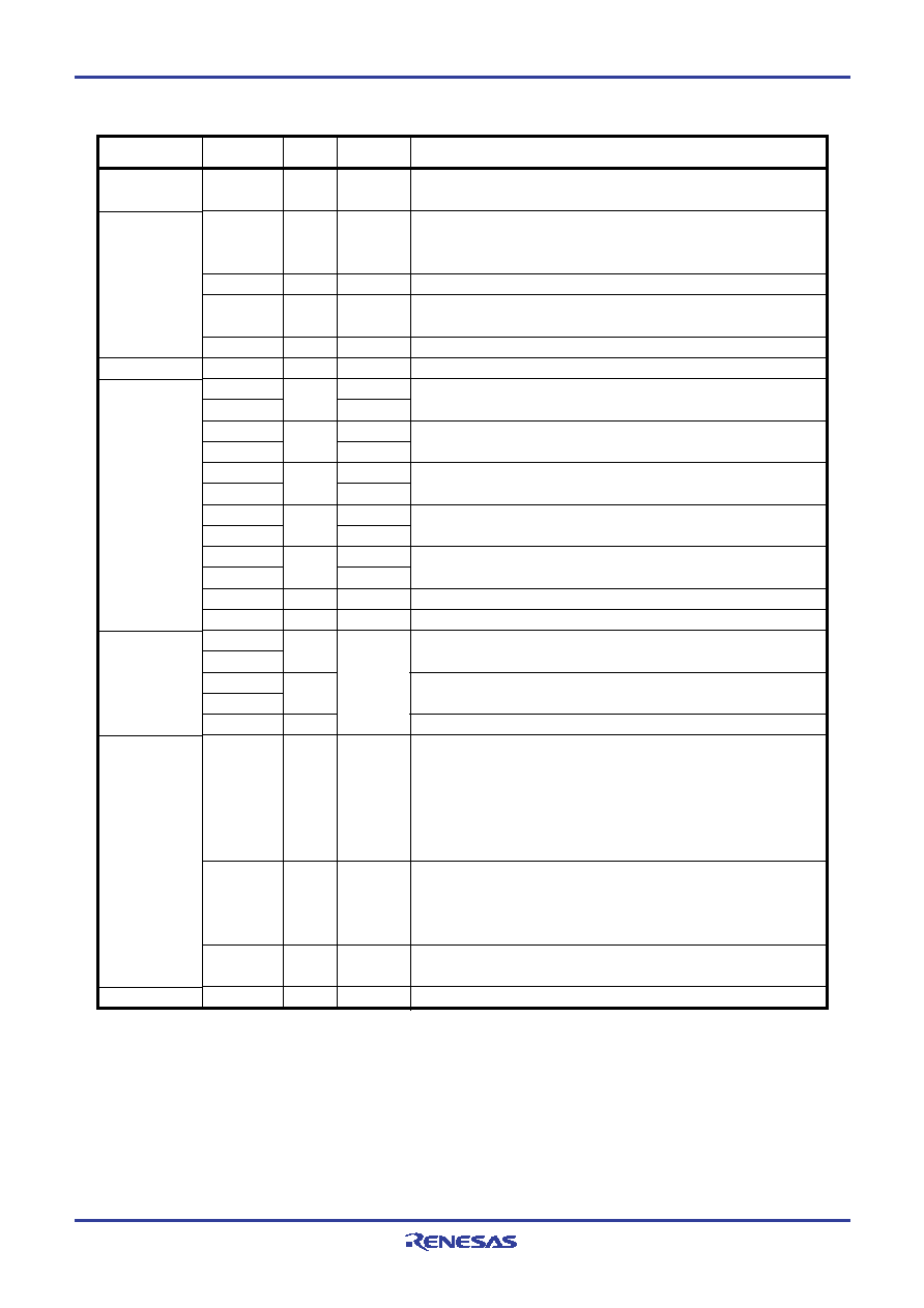
Reference
Voltage Input
A/D Converter
D/A Converter
Intelligent I/O
CAN
I/O Ports
Input Port
-
VCC1
VCC1/VCC2(1)
VCC1
VCC1/VCC2(1)
VCC1
VCC1/VCC2(1)
VCC1
VCC1/VCC2(1)
VCC1
VCC1/VCC2(1)
VCC1
VCC2
VCC1
Applies reference voltage to the A/D converter and D/A converter
Analog input pins for the A/D converter
Input pin for an external A/D trigger
Extended analog input pin for the A/D converter and output pin in
external op-amp connection mode
Extended analog input pin for the A/D converter
Output pin for the D/A converter
Input pins for the time measurement function
Output pins for the waveform generating function
(OUTC16 and OUTC17 assigned to P70 and P71 are pins for the N-channel open drain output.)
Inputs and outputs the clock for the intelligent I/O communication
function
Inputs data for the intelligent I/O communication function
Outputs data for the intelligent I/O communication function
Inputs data for the intelligent I/O communication function
Outputs data for the intelligent I/O communication function
Input pin for the CAN communication function
Output pin for the CAN communication function
Input pin for the CAN1 wake-up interrupt
I/O ports for CMOS. Each port can be programmed for input or
output under the control of the direction register. An input port
can be set, by program, for a pull-up resistor available or for no
pull-up resister available in 4-bit units
I/O ports having equivalent functions to P0
(P70 and P71 are ports for the N-channel open drain output.)
I/O ports having equivalent functions to P0
_______
Shares a pin with NMI. NMI input state can be got by reading P85
Supply
Classsfication
Symbol
I/O Type
Function
Voltage
I
I/O
I
O
I
O
I/O
I
O
I
O
I
O
I
I/O
I
I : Input
O : Output
I/O : Input and output
NOTES:
1. VCC2 is not available in the 100-pin package. VCC1 only available.
Table 1.6 Pin Description (100-Pin and 144-Pin Packages) (Continued)
相关PDF资料 |
PDF描述 |
|---|---|
| M32196F8TFP | 32-BIT, FLASH, 160 MHz, RISC MICROCONTROLLER, PQFP144 |
| M37546G2SP | 8-BIT, MROM, 8 MHz, MICROCONTROLLER, PDIP32 |
| M38047M8-XXXHP | 8-BIT, MROM, 8.4 MHz, MICROCONTROLLER, PQFP64 |
| M102E1000.0000DL | 1000 MHz, OTHER CLOCK GENERATOR, MDIP24 |
| M102P0200.0000DL | 200 MHz, OTHER CLOCK GENERATOR, MDIP24 |
相关代理商/技术参数 |
参数描述 |
|---|---|
| M30855FJGP | 制造商:RENESAS 制造商全称:Renesas Technology Corp 功能描述:SINGLE-CHIP 16/32-BIT CMOS MICROCOMPUTER |
| M30855FJGP#D3 | 制造商:Renesas Electronics Corporation 功能描述:MCU 16BIT R8C CISC 512KB FLASH 5V 144LQFP - Trays |
| M30855FJGP#D5 | 制造商:Renesas Electronics Corporation 功能描述:MCU 16BIT R8C CISC 512KB FLASH 5V 144LQFP - Trays |
| M30855FJGP#U3 | 功能描述:IC M32C MCU FLASH 512K 144LQFP RoHS:是 类别:集成电路 (IC) >> 嵌入式 - 微控制器, 系列:M16C™ M32C/80/85 标准包装:1 系列:AVR® ATmega 核心处理器:AVR 芯体尺寸:8-位 速度:16MHz 连通性:I²C,SPI,UART/USART 外围设备:欠压检测/复位,POR,PWM,WDT 输入/输出数:32 程序存储器容量:32KB(16K x 16) 程序存储器类型:闪存 EEPROM 大小:1K x 8 RAM 容量:2K x 8 电压 - 电源 (Vcc/Vdd):2.7 V ~ 5.5 V 数据转换器:A/D 8x10b 振荡器型:内部 工作温度:-40°C ~ 125°C 封装/外壳:44-TQFP 包装:剪切带 (CT) 其它名称:ATMEGA324P-B15AZCT |
| M30855FJGP#U5 | 功能描述:IC M32C MCU FLASH 512K 144LQFP RoHS:是 类别:集成电路 (IC) >> 嵌入式 - 微控制器, 系列:M16C™ M32C/80/85 标准包装:1 系列:AVR® ATmega 核心处理器:AVR 芯体尺寸:8-位 速度:16MHz 连通性:I²C,SPI,UART/USART 外围设备:欠压检测/复位,POR,PWM,WDT 输入/输出数:32 程序存储器容量:32KB(16K x 16) 程序存储器类型:闪存 EEPROM 大小:1K x 8 RAM 容量:2K x 8 电压 - 电源 (Vcc/Vdd):2.7 V ~ 5.5 V 数据转换器:A/D 8x10b 振荡器型:内部 工作温度:-40°C ~ 125°C 封装/外壳:44-TQFP 包装:剪切带 (CT) 其它名称:ATMEGA324P-B15AZCT |
发布紧急采购,3分钟左右您将得到回复。