- 您现在的位置:买卖IC网 > PDF目录80594 > M30878FJGP 32-BIT, FLASH, 32 MHz, MICROCONTROLLER, PQFP144 PDF资料下载
参数资料
| 型号: | M30878FJGP |
| 元件分类: | 微控制器/微处理器 |
| 英文描述: | 32-BIT, FLASH, 32 MHz, MICROCONTROLLER, PQFP144 |
| 封装: | 20 X 20 MM, 0.50 MM PITCH, PLASTIC, LQFP-144 |
| 文件页数: | 11/91页 |
| 文件大小: | 2390K |
| 代理商: | M30878FJGP |
第1页第2页第3页第4页第5页第6页第7页第8页第9页第10页当前第11页第12页第13页第14页第15页第16页第17页第18页第19页第20页第21页第22页第23页第24页第25页第26页第27页第28页第29页第30页第31页第32页第33页第34页第35页第36页第37页第38页第39页第40页第41页第42页第43页第44页第45页第46页第47页第48页第49页第50页第51页第52页第53页第54页第55页第56页第57页第58页第59页第60页第61页第62页第63页第64页第65页第66页第67页第68页第69页第70页第71页第72页第73页第74页第75页第76页第77页第78页第79页第80页第81页第82页第83页第84页第85页第86页第87页第88页第89页第90页第91页
1. Overview
Page 19 of 85
1.5
Pin Functions
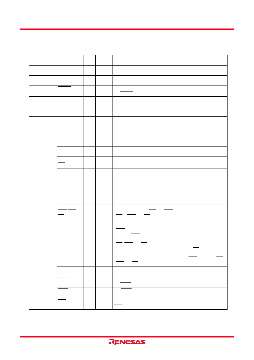
Table 1.15
Pin Functions (100-Pin and 144-Pin Packages) (1/4)
I: Input
O: Output I/O: Input and output
Type
Symbol
I/O
Type
Supply
Voltage
Description
Power supply
VCC1,VCC2
VSS
Apply 3.0 to 5.5 V to pins VCC1 and VCC2, and 0 V to the VSS pin.
The input condition of VCC1
≥ VCC2 must be met.
Analog power
supply input
AVCC
AVSS
VCC1
Power supply input pins to the A/D converter and D/A converter.
Connect the AVCC pin to VCC1, and the AVSS pin to VSS.
Reset input
RESET
I
VCC1
The MCU is placed in the reset state while applying an “L” signal to
the RESET pin.
CNVSS
I
VCC1
This pin switches processor mode. Apply an “L” to the CNVSS pin
to start up in single-chip mode, or an “H” to start up in
microprocessor mode (mask ROM, flash memory version) and boot
mode (flash memory version).
External data
bus width
select input
BYTE
I
VCC1
This pin switches a data bus width in external memory space 3. A
data bus is 16 bits wide when the BYTE pin is held “L” and 8 bits
wide when it is held “H”. Fix to either “L” or “H”.
Apply an “L” to the BYTE pin in single-chip mode.
Bus control
Pins
D0 to D7
I/O
VCC2
Data (D0 to D7) input/output pins while accessing an external
memory space with separate bus.
D8 to D15
I/O
VCC2
Data (D8 to D15) input/output pins while accessing an external
memory space with 16-bit separate bus.
A0 to A22
O
VCC2
Address bits (A0 to A22) output pins.
A23
O
VCC2
Inverted address bit (A23) output pin.
A0/D0 to
A7/D7
I/O
VCC2
Data (D0 to D7) input/output and 8 low-order address bits (A0 to
A7) output are performed by time-sharing these pins while
accessing an external memory space with multiplexed bus.
A8/D8 to
A15/D15
I/O
VCC2
Data (D8 to D15) input/output and 8 middle-order address bits (A8
to A15) output are performed by time-sharing these pins while
accessing an external memory space with 16-bit multiplexed bus.
CS0 to CS3
O
VCC2
Chip-select signal output pins used to specify external devices.
WRL/WR
WRH/BHE
RD
O
VCC2
WRL, WRH, (WR, BHE) and RD signal output pins. WRL and WRH
can be switched with WR and BHE by a program.
WRL, WRH and RD are selected:
If external data bus is 16 bits wide, data is written to an even
address in external memory space while an “L” is output from the
WRL pin. Data is written to an odd address while an “L” is output
from the WRH pin. Data is read while an “L” is output from the
RD pin.
WR, BHE and RD are selected:
Data is written while an “L” is output from the WR pin. Data is
read while an “L” is output from the RD pin. Data in odd address
is accessed while an “L” is output from the BHE pin. Select WR,
BHE and RD when an external data bus is 8 bits wide.
ALE
O
VCC2
ALE signal is used for the external devices to latch address signals
when the multiplexed bus is selected.
HOLD
I
VCC2
The MCU is placed in a hold state while an “L” signal is applied to
the HOLD pin.
HLDA
O
VCC2
The HLDA pin outputs an “L” while the MCU is placed in a hold
state.
RDY
I
VCC2
Bus is placed in a wait state while an “L” signal is applied to the
RDY pin.
相关PDF资料 |
PDF描述 |
|---|---|
| MC7448HX1420LD | 32-BIT, 1420 MHz, RISC PROCESSOR, CBGA360 |
| MPC8347ZUADF | 32-BIT, 266 MHz, RISC PROCESSOR, PBGA672 |
| MB90347CEPFV | 16-BIT, MROM, 24 MHz, MICROCONTROLLER, PQFP100 |
| MB90349CESPFV | 16-BIT, MROM, 24 MHz, MICROCONTROLLER, PQFP100 |
| MC68HC08QT1VDWE | 8-BIT, FLASH, 8 MHz, MICROCONTROLLER, PDSO8 |
相关代理商/技术参数 |
参数描述 |
|---|---|
| M30878FJGP#U3 | 功能描述:IC M32C/87 MCU FLASH 144LQFP RoHS:是 类别:集成电路 (IC) >> 嵌入式 - 微控制器, 系列:M16C™ M32C/80/87 标准包装:160 系列:S08 核心处理器:S08 芯体尺寸:8-位 速度:40MHz 连通性:I²C,LIN,SCI,SPI 外围设备:LCD,LVD,POR,PWM,WDT 输入/输出数:53 程序存储器容量:32KB(32K x 8) 程序存储器类型:闪存 EEPROM 大小:- RAM 容量:1.9K x 8 电压 - 电源 (Vcc/Vdd):2.7 V ~ 5.5 V 数据转换器:A/D 12x12b 振荡器型:内部 工作温度:-40°C ~ 105°C 封装/外壳:64-LQFP 包装:托盘 |
| M30878FJGP#U5 | 功能描述:IC M32C/87 MCU FLASH 144LQFP RoHS:是 类别:集成电路 (IC) >> 嵌入式 - 微控制器, 系列:M16C™ M32C/80/87 标准包装:160 系列:S08 核心处理器:S08 芯体尺寸:8-位 速度:40MHz 连通性:I²C,LIN,SCI,SPI 外围设备:LCD,LVD,POR,PWM,WDT 输入/输出数:53 程序存储器容量:32KB(32K x 8) 程序存储器类型:闪存 EEPROM 大小:- RAM 容量:1.9K x 8 电压 - 电源 (Vcc/Vdd):2.7 V ~ 5.5 V 数据转换器:A/D 12x12b 振荡器型:内部 工作温度:-40°C ~ 105°C 封装/外壳:64-LQFP 包装:托盘 |
| M30878MJA-XXXGP | 制造商:RENESAS 制造商全称:Renesas Technology Corp 功能描述:RENESAS MCU |
| M30878MJB-XXXGP | 制造商:RENESAS 制造商全称:Renesas Technology Corp 功能描述:RENESAS MCU |
| M30878MJ-XXXGP | 制造商:RENESAS 制造商全称:Renesas Technology Corp 功能描述:RENESAS MCU |
发布紧急采购,3分钟左右您将得到回复。