- 您现在的位置:买卖IC网 > PDF目录383294 > M312L2920BG0-CB3 (SAMSUNG SEMICONDUCTOR CO. LTD.) DDR SDRAM Registered Module PDF资料下载
参数资料
| 型号: | M312L2920BG0-CB3 |
| 厂商: | SAMSUNG SEMICONDUCTOR CO. LTD. |
| 英文描述: | DDR SDRAM Registered Module |
| 中文描述: | DDR SDRAM的注册模块 |
| 文件页数: | 13/23页 |
| 文件大小: | 258K |
| 代理商: | M312L2920BG0-CB3 |
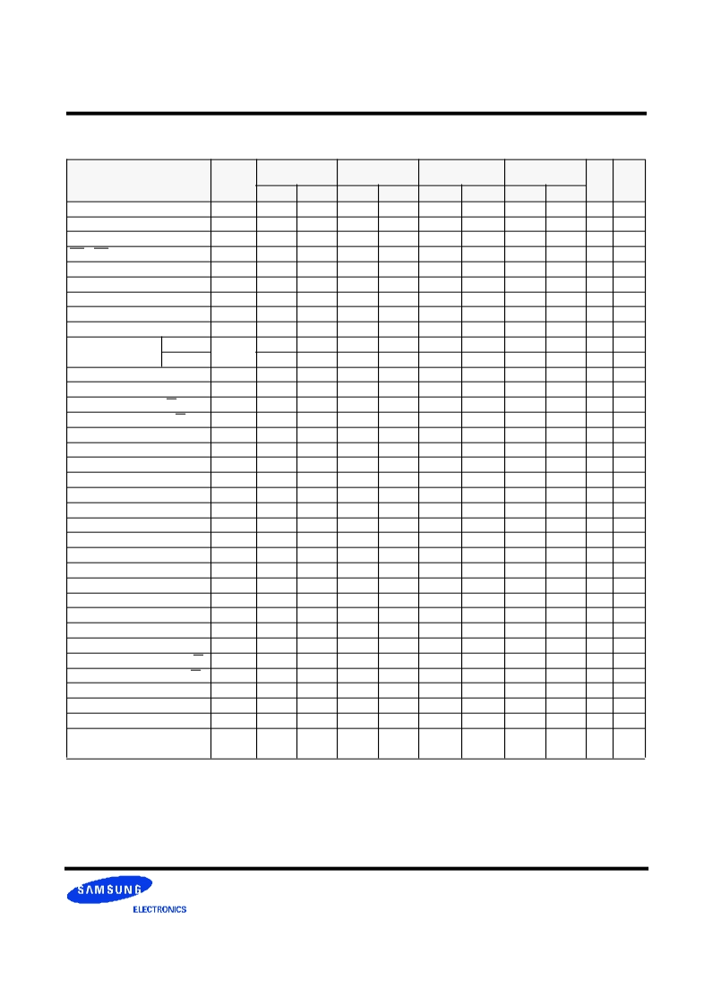
DDR SDRAM
512MB, 1GB, 2GB TSOP Registered DIMM
Revison 1.0 December, 2003
AC Timming Parameters & Specifications
Parameter
Symbol
AA
(DDR266@CL=2)
A2
(DDR266@CL=2)
B0
(DDR266@CL=2.5)
A0
(DDR200@CL=2)
Unit
Note
Mn
Max
Min
Max
Mn
Max
Min
Max
Row cycle time
tRC
60
65
65
70
ns
Refresh row cycle time
tRFC
75
75
75
80
ns
Row active time
tRAS
45
120K
45
120K
45
120K
48
120K
ns
RAS to CAS delay
tRCD
15
20
20
20
ns
Row precharge time
tRP
15
20
20
20
ns
Row active to Row active delay
tRRD
15
15
15
15
ns
Write recovery time
tWR
15
15
15
15
ns
Last data in to Read command
tWTR
1
1
1
1
tCK
Col. address to Col. address delay
tCCD
1
1
1
1
tCK
Clock cycle time
CL=2.0
tCK
7.5
12
7.5
12
10
12
10
12
ns
CL=2.5
7.5
12
7.5
12
7.5
12
ns
Clock high level width
tCH
0.45
0.55
0.45
0.55
0.45
0.55
0.45
0.55
tCK
Clock low level width
tCL
0.45
0.55
0.45
0.55
0.45
0.55
0.45
0.55
tCK
DQS-out access time fromCK/CK
tDQSCK
-0.75
+0.75
-0.75
+0.75
-0.75
+0.75
-0.8
+0.8
ns
Output data access time fromCK/CK
tAC
-0.75
+0.75
-0.75
+0.75
-0.75
+0.75
-0.8
+0.8
ns
Data strobe edge to ouput data edge
tDQSQ
-
0.5
-
0.5
-
0.5
-
0.6
ns
12
Read Preamble
tRPRE
0.9
1.1
0.9
1.1
0.9
1.1
0.9
1.1
tCK
Read Postamble
tRPST
0.4
0.6
0.4
0.6
0.4
0.6
0.4
0.6
tCK
CK to valid DQS-in
tDQSS
0.75
1.25
0.75
1.25
0.75
1.25
0.75
1.25
tCK
DQS-in setup time
tWPRES
0
0
0
0
ns
3
DQS-in hold time
tWPRE
0.25
0.25
0.25
0.25
tCK
DQS falling edge to CK rising-setup time
tDSS
0.2
0.2
0.2
0.2
tCK
DQS falling edge fromCK rising-hold time
tDSH
0.2
0.2
0.2
0.2
tCK
DQS-in high level width
tDQSH
0.35
0.35
0.35
0.35
tCK
DQS-in low level width
tDQSL
0.35
0.35
0.35
0.35
tCK
DQS-in cycle time
tDSC
0.9
1.1
0.9
1.1
0.9
1.1
0.9
1.1
tCK
Address and Control Input setup time(fast)
tIS
0.9
0.9
0.9
1.1
ns
i,5.7~9
Address and Control Input hold time(fast)
tIH
0.9
0.9
0.9
1.1
ns
i,5.7~9
Address and Control Input setup time(slow)
tIS
1.0
1.0
1.0
1.1
ns
i, 6~9
Address and Control Input hold time(slow)
tIH
1.0
1.0
1.0
1.1
ns
i, 6~9
Data-out high impedence time fromCK/CK
tHZ
-0.75
+0.75
-0.75
+0.75
-0.75
+0.75
-0.8
+0.8
ns
1
Data-out low impedence time fromCK/CK
tLZ
-0.75
+0.75
-0.75
+0.75
-0.75
+0.75
-0.8
+0.8
ns
1
Input Slew Rate(for input only pins)
tSL(I)
0.5
0.5
0.5
0.5
V/ns
Input Slew Rate(for I/O pins)
tSL(IO)
0.5
0.5
0.5
0.5
V/ns
Output Slew Rate(x4,x8)
tSL(O)
1.0
4.5
1.0
4.5
1.0
4.5
1.0
4.5
V/ns
Output Slew Rate Matching Ratio
(rise to
fall)
tSLMR
0.67
1.5
0.67
1.5
0.67
1.5
0.67
1.5
相关PDF资料 |
PDF描述 |
|---|---|
| M312L5628BT0-A2 | DDR SDRAM Registered Module |
| M312L5628BT0-CAA | DDR SDRAM Registered Module |
| M312L6523BTS-A2 | DDR SDRAM Registered Module |
| M312L6523BTS-CAA | DDR SDRAM Registered Module |
| M312L5720BG0-A2 | DDR SDRAM Registered Module |
相关代理商/技术参数 |
参数描述 |
|---|---|
| M312L2920BT | 制造商:SAMSUNG 制造商全称:Samsung semiconductor 功能描述:DDR SDRAM Registered Module |
| M312L2920BTS-A2 | 制造商:SAMSUNG 制造商全称:Samsung semiconductor 功能描述:DDR SDRAM Registered Module |
| M312L2920BTS-CAA | 制造商:SAMSUNG 制造商全称:Samsung semiconductor 功能描述:DDR SDRAM Registered Module |
| M312L2920CZ3-CB300 | 制造商:Samsung Semiconductor 功能描述:512MSDDDR_MDDR SDRAM MODULX72BOC(LF) - Bulk |
| M312L2920DUS | 制造商:SAMSUNG 制造商全称:Samsung semiconductor 功能描述:DDR SDRAM Product Guide |
发布紧急采购,3分钟左右您将得到回复。