- 您现在的位置:买卖IC网 > PDF目录69010 > M34508G4HFP 4-BIT, MROM, 6 MHz, MICROCONTROLLER, PDSO20 PDF资料下载
参数资料
| 型号: | M34508G4HFP |
| 元件分类: | 微控制器/微处理器 |
| 英文描述: | 4-BIT, MROM, 6 MHz, MICROCONTROLLER, PDSO20 |
| 封装: | 5.30 X12.60 MM, 1.27 MM PITCH, PLASTIC, SOP-20 |
| 文件页数: | 6/32页 |
| 文件大小: | 1049K |
| 代理商: | M34508G4HFP |
第1页第2页第3页第4页第5页当前第6页第7页第8页第9页第10页第11页第12页第13页第14页第15页第16页第17页第18页第19页第20页第21页第22页第23页第24页第25页第26页第27页第28页第29页第30页第31页第32页
Rev.1.03
2009.07.27
page 14 of 140
REJ03B0148-0103
4508 Group
FUNCTION BLOCK OPERATIONS
CPU
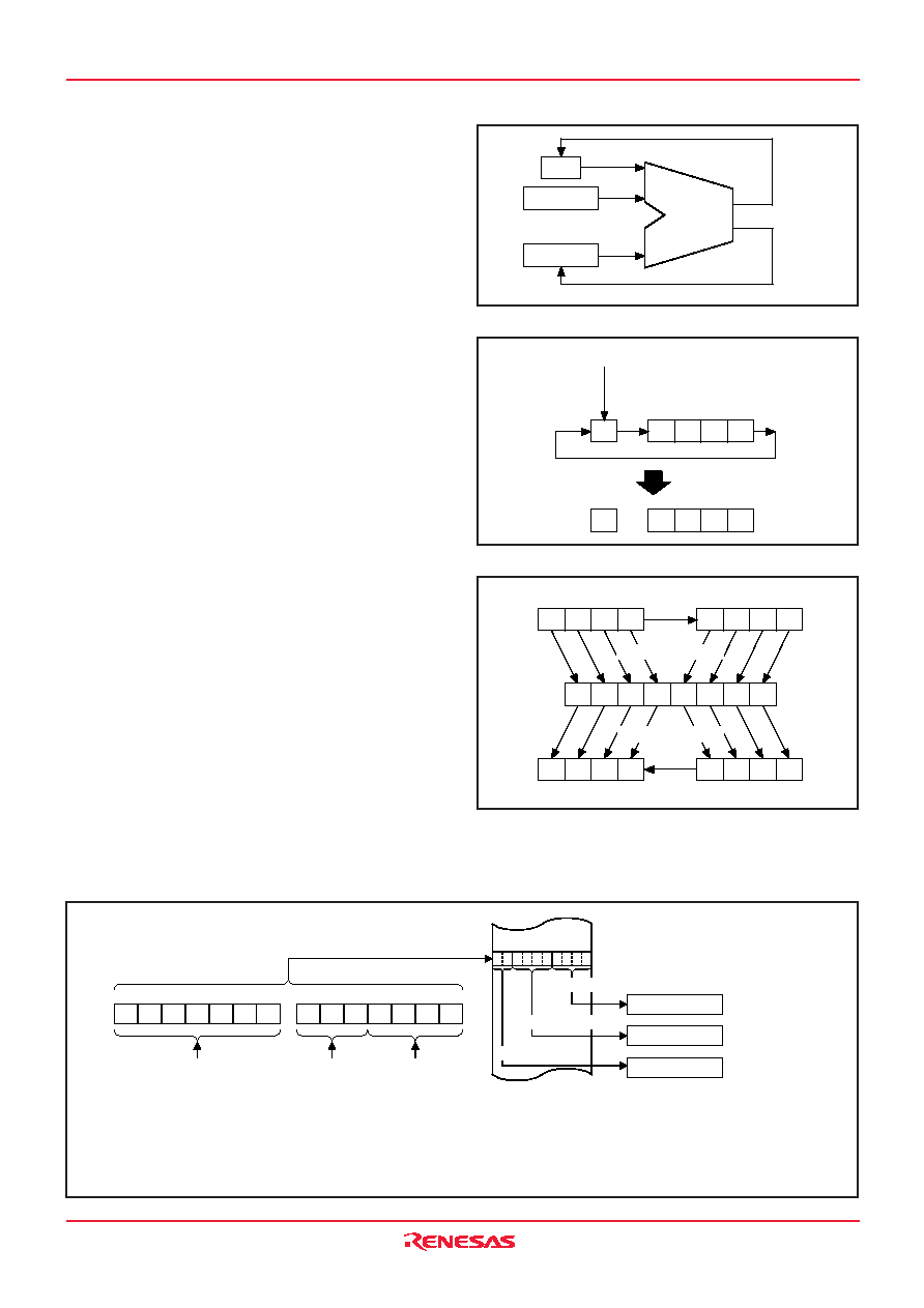
(1) Arithmetic logic unit (ALU)
The arithmetic logic unit ALU performs 4-bit arithmetic such as 4-bit
data addition, comparison, AND operation, OR operation, and bit
manipulation.
(2) Register A and carry flag
Register A is a 4-bit register used for arithmetic, transfer, exchange,
and I/O operation.
Carry flag CY is a 1-bit flag that is set to “1” when there is a carry
with the AMC instruction (Figure 1).
It is unchanged with both A n instruction and AM instruction. The
value of A0 is stored in carry flag CY with the RAR instruction (Figure
2).
Carry flag CY can be set to “1” with the SC instruction and cleared to
“0” with the RC instruction.
(3) Registers B and E
Register B is a 4-bit register used for temporary storage of 4-bit data,
and for 8-bit data transfer together with register A.
Register E is an 8-bit register. It can be used for 8-bit data transfer
with register B used as the high-order 4 bits and register A as the
low-order 4 bits (Figure 3).
Register E is undefined after system is released from reset and re-
turned from the RAM back-up. Accordingly, set the initial value.
(4) Register D
Register D is a 3-bit register.
It is used to store a 7-bit ROM address together with register A and
is used as a pointer within the specified page when the TABP p, BLA
p, or BMLA p instruction is executed (Figure 4).
Also, when the TABP p instruction is executed at UPTF flag = “1”,
the high-order 2 bits of ROM reference data is stored to the low-or-
der 2 bits of register D, the high-order 1 bit of register D is “0”. When
the TABP p instruction is executed at UPTF flag = “0”, the contents
of register D remains unchanged. The UPTF flag is set to “1” with the
SUPT instruction and cleared to “0” with the RUPT instruction. The
initial value of UPTF flag is “0”.
Register D is undefined after system is released from reset and re-
turned from the RAM back-up. Accordingly, set the initial value.
Fig. 1 AMC instruction execution example
Fig. 2 RAR instruction execution example
Fig. 3 Registers A, B and register E
Fig. 4 TABP p instruction execution example
(CY)
(M(DP))
(A)
Addition
ALU
<Carry>
<Result>
A3 A2 A1 A0
B3 B2 B1 B0
E7 E6 E5 E4 E3 E2 E1 E0
A3 A2 A1 A0
B3 B2 B1 B0
TAB instruction
TEAB instruction
TABE instruction
TBA instruction
Register BRegister A
Register B
Register A
Register E
CY
A3 A2 A1 A0
A0
CY A3 A2 A1
<Rotation>
RAR instruction
<Set>
SC instruction
<Clear>
RC instruction
Specifying address
TABP p instruction
p6 p5 p4
p3 p2 p1 p0
PCH
DR2DR1DR0 A3 A2 A1 A0
PCL
Immediate field
value p
The contents of
register D
ROM
84
0
Middle-order 4 bits
Low-order 4bits
Register A (4)
Register B (4)
The contents of
register A
High-order 2 bits
Register D (3)
* Flag UPTF = 1;
High-order
2
bits
of
reference
data
is
transferred to the low-order 2 bits of register D.
“0” is stored to the high-order 1 bit of register D.
Flag UPTF = 0;
Data is not transferred to register D.
相关PDF资料 |
PDF描述 |
|---|---|
| M34508G4GP | 4-BIT, MROM, 6 MHz, MICROCONTROLLER, PDSO20 |
| M34508G4H-XXXFP | 4-BIT, MROM, 6 MHz, MICROCONTROLLER, PDSO20 |
| M34508G4-XXXFP | 4-BIT, MROM, 6 MHz, MICROCONTROLLER, PDSO20 |
| M34508G4FP | 4-BIT, MROM, 6 MHz, MICROCONTROLLER, PDSO20 |
| M34508G4-XXXGP | 4-BIT, MROM, 6 MHz, MICROCONTROLLER, PDSO20 |
相关代理商/技术参数 |
参数描述 |
|---|---|
| M34508G4HGP | 制造商:RENESAS 制造商全称:Renesas Technology Corp 功能描述:SINGLE-CHIP 4-BIT CMOS MICROCOMPUTER |
| M34508G4H-XXXFP | 制造商:RENESAS 制造商全称:Renesas Technology Corp 功能描述:SINGLE-CHIP 4-BIT CMOS MICROCOMPUTER |
| M34508G4H-XXXGP | 制造商:RENESAS 制造商全称:Renesas Technology Corp 功能描述:SINGLE-CHIP 4-BIT CMOS MICROCOMPUTER |
| M34508G4-XXXFP | 制造商:RENESAS 制造商全称:Renesas Technology Corp 功能描述:SINGLE-CHIP 4-BIT CMOS MICROCOMPUTER |
| M34508G4-XXXGP | 制造商:RENESAS 制造商全称:Renesas Technology Corp 功能描述:SINGLE-CHIP 4-BIT CMOS MICROCOMPUTER |
发布紧急采购,3分钟左右您将得到回复。