- 您现在的位置:买卖IC网 > PDF目录67761 > M34553G8HFP 4-BIT, OTPROM, 6 MHz, MICROCONTROLLER, PQFP48 PDF资料下载
参数资料
| 型号: | M34553G8HFP |
| 元件分类: | 微控制器/微处理器 |
| 英文描述: | 4-BIT, OTPROM, 6 MHz, MICROCONTROLLER, PQFP48 |
| 封装: | 7 X 7 MM, 0.50 MM PITCH, PLASTIC, LQFP-48 |
| 文件页数: | 9/13页 |
| 文件大小: | 1058K |
| 代理商: | M34553G8HFP |
Rev.3.02
Dec 22, 2006
page 5 of 142
REJ03B0024-0302
4553 Group
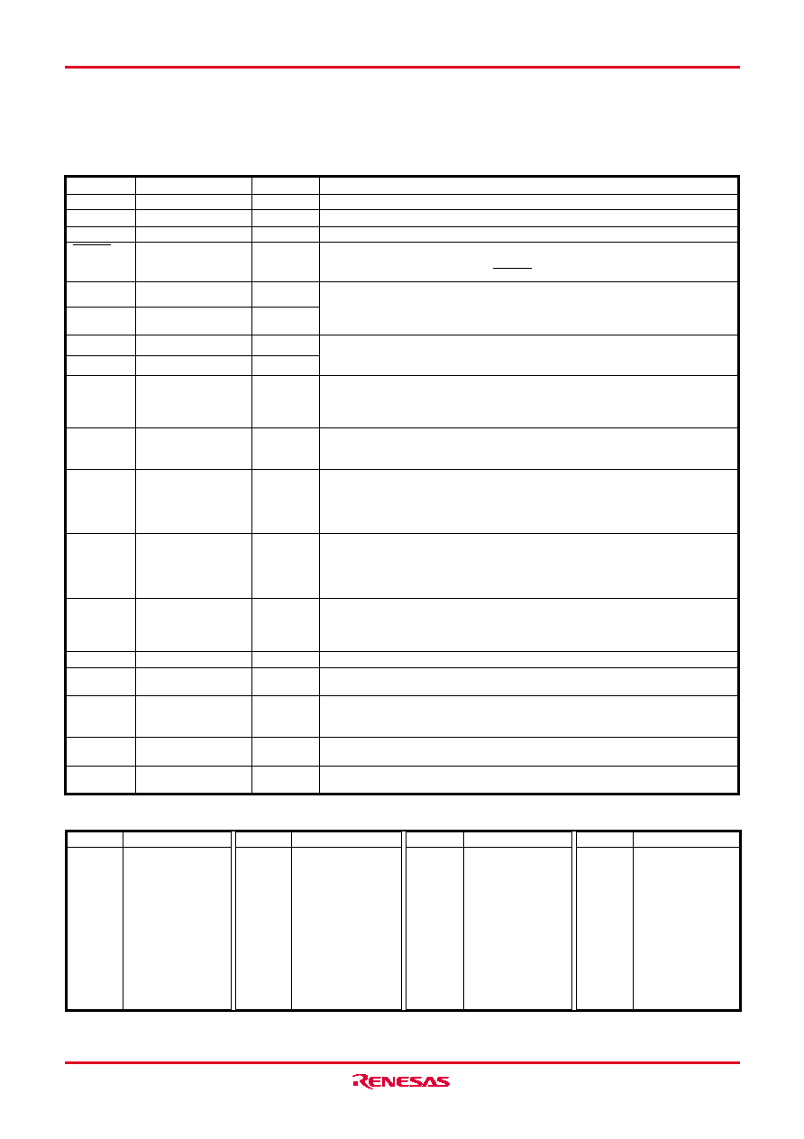
PIN DESCRIPTION
Name
Power supply
Ground
CNVSS
Reset input/output
Main clock input
Sub-clock input
Pin
VDD
VSS
CNVSS
RESET
XIN
XCIN
Input/Output
—
I/O
Input
Function
Connected to a plus power supply.
Connected to a 0 V power supply.
Connect CNVSS to VSS and apply “L” (0V) to CNVSS certainly.
An N-channel open-drain I/O pin for a system reset. When the SRST instruction,
watchdog timer, the built-in power-on reset or the voltage drop detection circuit
causes the system to be reset, the RESET pin outputs “L” level.
I/O pins of the main clock generating circuit. When using a ceramic resonator, con-
nect it between pins XIN and XOUT. A feedback resistor is built-in between them.
When using the RC oscillation, connect a resistor and a capacitor to XIN, and leave
XOUT pin open.
I/O pins of the sub-clock generating circuit. Connect a 32.768 kHz quartz-crystal oscilla-
tor between pins XCIN and XCOUT. A feedback resistor is built-in between them. XCIN and
XCOUT pins are also used as ports D6 and D7, respectively.
XOUT
Main clock output
Output
D0–D5
D6, D7
P00–P03
P10–P13
P20–P23
Port C
COM0–
COM3
SEG0–SEG28
CNTR
INT
I/O port D
Input is examined by
skip decision.
Output port D
I/O port P0
I/O port P1
I/O port P2
Output port C
Common output
Segment output
Timer input/output
Interrupt input
I/O
Output
I/O
Output
I/O
Input
Each pin of port D has an independent 1-bit wide I/O function. The output structure
can be switched to N-channel open-drain or CMOS by software. For input use, set
the latch of the specified bit to “1” and select the N-channel open-drain. Port D5 is
also used as INT pin.
Each pin of port D has an independent 1-bit wide output function. The output struc-
ture is N-channel open-drain. Ports D6 and D7 are also used as XCIN pin and XCOUT
pin, respectively.
Port P0 serves as a 4-bit I/O port. The output structure can be switched to N-channel
open-drain or CMOS by software. For input use, set the latch of the specified bit to
“1” and select the N-channel open-drain. Port P0 has a key-on wakeup function and
a pull-up function. Both functions can be switched by software. Ports P00–P03 are
also used as SEG21–SEG24, respectively.
Port P1 serves as a 4-bit I/O port. The output structure can be switched to N-channel
open-drain or CMOS by software. For input use, set the latch of the specified bit to
“1” and select the N-channel open-drain. Port P1 has a key-on wakeup function and
a pull-up function. Both functions can be switched by software. Ports P10–P13 are
also used as SEG25–SEG28, respectively.
Port P2 serves as a 4-bit I/O port. The output structure can be switched to N-channel
open-drain or CMOS by software. For input use, set the latch of the specified bit to
“1” and select the N-channel open-drain.
Ports P20–P23 are also used as SEG17–SEG20, respectively.
1-bit output port. The output structure is CMOS. Port C is also used as CNTR pin.
LCD common output pins. Pins COM0 and COM1 are used at 1/2 duty, pins COM0–
COM2 are used at 1/3 duty and pins COM0–COM3 are used at 1/4 duty.
LCD segment output pins. SEG0–SEG2 pins are used as VLC3–VLC1 pins, respec-
tively. SEG17–SEG28 pins are used as Ports P20–P23, Ports P00–P03 and Ports
P10–P13, respectively.
CNTR pin has the function to input the clock for the timer 1 event counter and to out-
put the PWM signal generated by timer 2.CNTR pin is also used as Port C.
INT pin accepts external interrupts. They have the key-on wakeup function which can
be switched by software. INT pin is also used as Port D5.
Notes 1: Pins except above have just single function.
2: The input/output of D5 can be used even when INT is selected.
The threshold value is different between port D5 and INT. Accordingly, be careful when the input of both is used.
3: The port C “H” output function can be used even when CNTR (output) is selected.
Pin
XCIN
XCOUT
P00
P01
P02
P03
P10
P11
P12
P13
Multifunction
D6
D7
SEG21
SEG22
SEG23
SEG24
SEG25
SEG26
SEG27
SEG28
MULTIFUNCTION
Pin
D6
D7
SEG21
SEG22
SEG23
SEG24
SEG25
SEG26
SEG27
SEG28
Multifunction
XCIN
XCOUT
P00
P01
P02
P03
P10
P11
P12
P13
Pin
P20
P21
P22
P23
D5
C
SEG0
SEG1
SEG2
Multifunction
SEG17
SEG18
SEG19
SEG20
INT
CNTR
VLC3
VLC2
VLC1
Pin
SEG17
SEG18
SEG19
SEG20
INT
CNTR
VLC3
VLC2
VLC1
Multifunction
P20
P21
P22
P23
D5
C
SEG0
SEG1
SEG2
XCOUT
Sub-clock output
Output
相关PDF资料 |
PDF描述 |
|---|---|
| M34553M4H-XXXFP | 4-BIT, MROM, 6 MHz, MICROCONTROLLER, PQFP48 |
| M34553M8-XXXFP | 4-BIT, MROM, 6 MHz, MICROCONTROLLER, PQFP48 |
| M34554EDFP | 4-BIT, OTPROM, 6 MHz, MICROCONTROLLER, PQFP64 |
| M34554MC-XXXFP | 4-BIT, MROM, 6 MHz, MICROCONTROLLER, PQFP64 |
| M34556M4H-XXXFP | 4-BIT, MROM, 6 MHz, MICROCONTROLLER, PDSO42 |
相关代理商/技术参数 |
参数描述 |
|---|---|
| M34553M4H-XXXFP | 制造商:RENESAS 制造商全称:Renesas Technology Corp 功能描述:SINGLE-CHIP 4-BIT CMOS MICROCOMPUTER |
| M34553M4-XXXFP | 制造商:RENESAS 制造商全称:Renesas Technology Corp 功能描述:SINGLE-CHIP 4-BIT CMOS MICROCOMPUTER |
| M34553M8H-XXXFP | 制造商:RENESAS 制造商全称:Renesas Technology Corp 功能描述:SINGLE-CHIP 4-BIT CMOS MICROCOMPUTER |
| M34553M8-XXXFP | 制造商:RENESAS 制造商全称:Renesas Technology Corp 功能描述:SINGLE-CHIP 4-BIT CMOS MICROCOMPUTER |
| M34553MXH-XXXFP | 制造商:RENESAS 制造商全称:Renesas Technology Corp 功能描述:SINGLE-CHIP 4-BIT CMOS MICROCOMPUTER |
发布紧急采购,3分钟左右您将得到回复。